ADM2483BRW Просмотр технического описания (PDF) - Analog Devices
Номер в каталоге
Компоненты Описание
Список матч
ADM2483BRW Datasheet PDF : 20 Pages
| |||
Data Sheet
FEATURES
RS-485 transceiver with electrical data isolation
Complies with ANSI TIA/EIA RS-485-A and ISO 8482: 1987(E)
500 kbps data rate
Slew rate-limited driver outputs
Low power operation: 2.5 mA max
Suitable for 5 V or 3 V operations (VDD1)
High common-mode transient immunity: >25 kV/μs
True fail-safe receiver inputs
Chatter-free power-up/power-down protection
256 nodes on bus
Thermal shutdown protection
Safety and regulatory approvals
UL recognition: 2500 V rms for 1 minute per UL 1577
CSA Component Acceptance Notice #5A
IEC 609501 800 V rms (basic), 400 V rms (reinforced)
VDE Certificate of Conformity
DIN V VDE V 0884-10 (VDE V 0884-10): 2006-12
VIORM = 560 V peak
Operating temperature range: −40°C to +85°C
APPLICATIONS
Low power RS-485/RS-422 networks
Isolated interfaces
Building control networks
Multipoint data transmission systems
GENERAL DESCRIPTION
The ADM2483 differential bus transceiver is an integrated,
galvanically isolated component designed for bidirectional data
communication on balanced, multipoint bus transmission lines.
It complies with ANSI EIA/TIA-485-A and ISO 8482: 1987(E).
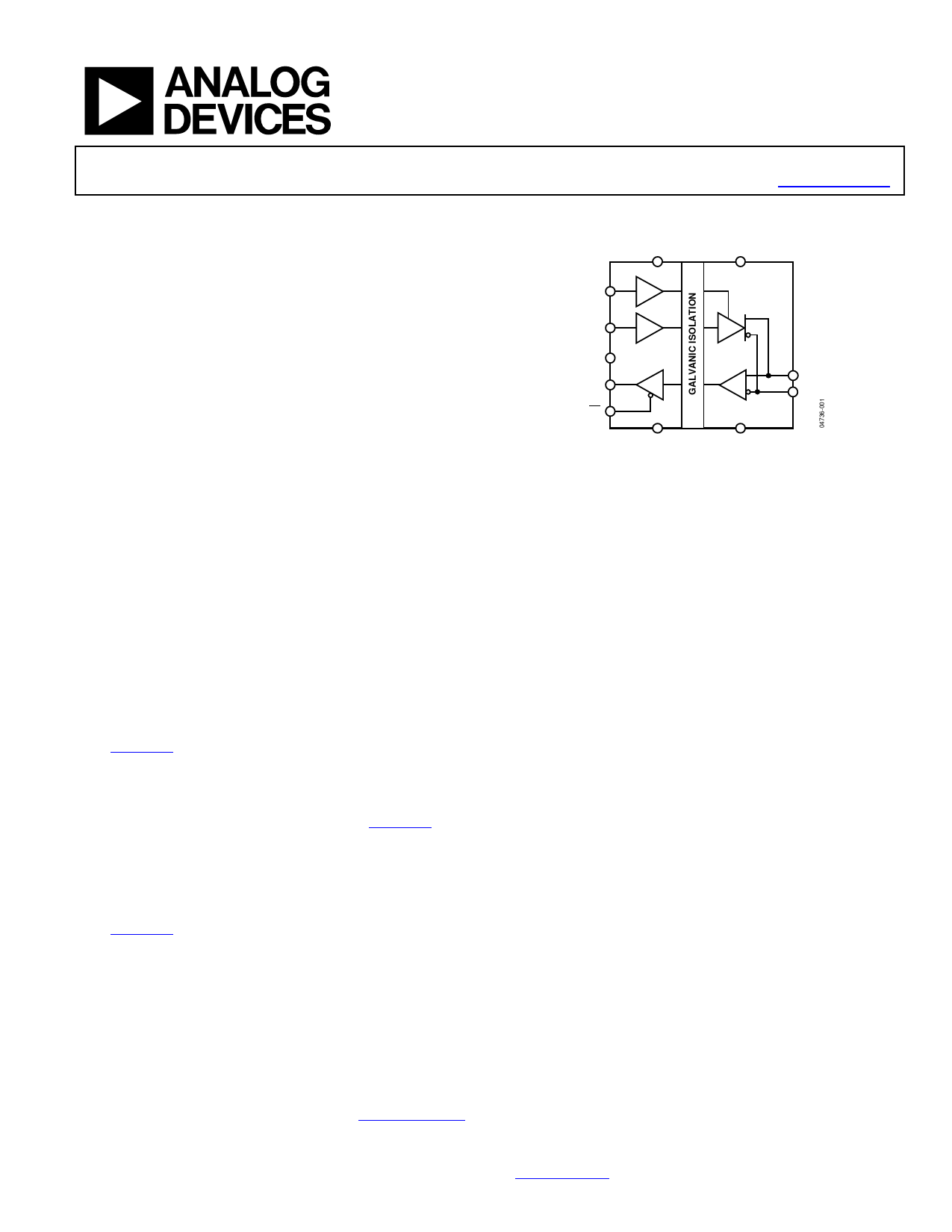
Using Analog Devices’ iCoupler technology, the ADM2483
combines a 3-channel isolator, a three-state differential line
driver, and a differential input receiver into a single package.
The logic side of the device is powered with either a 5 V or 3 V
supply, and the bus side uses a 5 V supply only.
The ADM2483 is slew-limited to reduce reflections with
improperly terminated transmission lines. The controlled slew
rate limits the data rate to 500 kbps. The device’s input impedance
is 96 kΩ, allowing up to 256 transceivers on the bus. Its driver
has an active-high enable feature. The driver differential outputs
Half-Duplex, iCoupler®
Isolated RS-485 Transceiver
ADM2483
FUNCTIONAL BLOCK DIAGRAM
VDD1
VDD2
ADM2483
DE
TxD
PV
A
RxD
B
RE
GND1
GND2
Figure 1.
and receiver differential inputs are connected internally to form
a differential I/O port. When the driver is disabled or when
VDD1 or VDD2 = 0 V, this imposes minimal loading on the bus.
An active-high receiver disable feature, which causes the receive
output to enter a high impedance state, is provided as well.
The receiver inputs have a true fail-safe feature that ensures a
logic-high receiver output level when the inputs are open or
shorted. This guarantees that the receiver outputs are in a
known state before communication begins and at the point
when communication ends.
Current limiting and thermal shutdown features protect against
output short circuits and bus contention situations that might
cause excessive power dissipation. The part is fully specified
over the industrial temperature range and is available in a
16-lead, wide body SOIC package.
Rev. C
Document Feedback
Information furnished by Analog Devices is believed to be accurate and reliable. However, no
responsibility is assumed by Analog Devices for its use, nor for any infringements of patents or other
rights of third parties that may result from its use. Specifications subject to change without notice. No
license is granted by implication or otherwise under any patent or patent rights of Analog Devices.
Trademarks and registered trademarks are the property of their respective owners.
One Technology Way, P.O. Box 9106, Norwood, MA 02062-9106, U.S.A.
Tel: 781.329.4700 ©2004–2013 Analog Devices, Inc. All rights reserved.
Technical Support
www.analog.com
Share Link: 