AD9245(RevE) Просмотр технического описания (PDF) - Analog Devices
Номер в каталоге
Компоненты Описание
Список матч
AD9245 Datasheet PDF : 32 Pages
| |||
Data Sheet
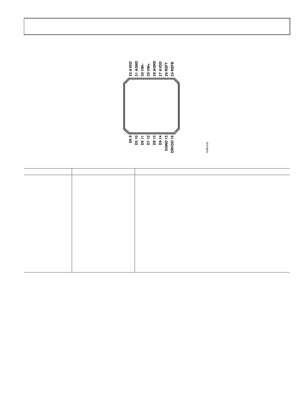
PIN CONFIGURATION AND FUNCTION DESCRIPTIONS
AD9245
DNC 1
CLK 2
DNC 3
PDWN 4
(LSB) D0 5
D1 6
D2 7
D3 8
AD9245
TOP VIEW
(Not to Scale)
24 VREF
23 SENSE
22 MODE
21 OTR
20 D13 (MSB)
19 D12
18 D11
17 D10
NOTES
1. DNC = DO NOT CONNECT. DO NOT CONNECT TO THIS PIN.
2. IT IS RECOMMENDED THAT THE EXPOSED PADDLE BE SOLDERED TO THE GROUND PLANE
FOR THE LFCSP PACKAGE. THERE IS AN INCREASED RELIABILITY OF THE SOLDER JOINTS,
AND THE MAXIMUM THERMAL CAPABILITY OF THE PACKAGE IS ACHIEVED WITH THE
EXPOSED PADDLE SOLDERED TO THE CUSTOMER BOARD.
Figure 3. LFCSP Pin Configuration
Table 9. Pin Function Descriptions
Pin No.
Mnemonic
1, 3
DNC
2
CLK
4
PDWN
5 to 14, 17 to 20
D0 (LSB) to D13 (MSB)
15
DGND
16
DRVDD
21
OTR
22
MODE
23
SENSE
24
VREF
25
REFB
26
REFT
27, 32
AVDD
28, 31
AGND
29
VIN+
30
VIN–
EPAD
Description
Do Not Connect
Clock Input Pin
Power-Down Function Select
Data Output Bits
Digital Output Ground
Digital Output Driver Supply
Out-of-Range Indicator
Data Format Select and DCS Mode Selection (See Table 11)
Reference Mode Selection (See Table 10)
Voltage Reference Input/Output
Differential Reference (–)
Differential Reference (+)
Analog Power Supply
Analog Ground
Analog Input Pin (+)
Analog Input Pin (–)
Exposed Pad. It is recommended that the exposed paddle be soldered to the ground
plane for the LFCSP package. There is an increased reliability of the solder joints, and
the maximum thermal capability of the package is achieved with the exposed paddle
soldered to the customer board.
Rev. E | Page 11 of 32
Share Link: 