AD8387 Просмотр технического описания (PDF) - Analog Devices
Номер в каталоге
Компоненты Описание
Список матч
AD8387 Datasheet PDF : 16 Pages
| |||
ABSOLUTE MAXIMUM RATINGS
Table 2.
Parameter
Rating
Supply Voltages
AVCCx − AGNDx
DVCC − DGND
Input Voltages
Maximum Digital Input Voltage
Minimum Digital Input Voltage
Maximum Analog Input Voltage
Minimum Analog Input Voltage
Internal Power Dissipation1
TQFP E-Pad @ TA = 25°C
Operating Temperature Range
Storage Temperature Range
Lead Temperature Range (Soldering 10 sec)
18 V
4.5 V
DVCC + 0.5 V
DGND − 0.5 V
AVCC + 0.5 V
AGND − 0.5 V
4.38 W
0°C to 85°C
−65°C to +125°C
300°C
1 80-lead TQFP E-Pad:
θJA = 28.5°C/W (still air) [JEDEC Standard, 4-layer PCB in still air]
θJC = 12.2°C/W
θJB = 14.6°C/W
ΨJB = 12.0°C/W
ΨJT = 0.3°C/W.
Stresses above those listed under the Absolute Maximum
Ratings may cause permanent damage to the device. This is a
stress rating only; functional operation of the device at these or
any other conditions above those indicated in the operational
section of this specification is not implied. Exposure to the
absolute maximum ratings for extended periods may reduce
device reliability.
EXPOSED PADDLE
To ensure optimized thermal performance, the exposed paddle
must be thermally connected to an external plane, such as
AVCC or GND, as described in the Applications section.
OVERLOAD PROTECTION
The AD8387 overload protection circuit consists of an output
current limiter and a thermal switch.
When TSW is LOW, the thermal switch is disabled and the
output current limiter is enabled. The maximum current at any
one output is internally limited to 100 mA average. In the event
of a momentary short-circuit between a video output and a
power supply rail (VCC or AGND), the output current limit is
sufficiently low to provide temporary protection.
AD8387
When TSW is HIGH, the output current limiter, as well as the
thermal switch, is enabled. The thermal switch debiases the
output amplifier when the junction temperature reaches the
internally set trip point. In the event of an extended short-
circuit between a video output and a power supply rail, the
output amplifier current continues to switch between 0 and
100 mA typical with a period determined by the thermal time
constant and the hysteresis of the thermal trip point. The
thermal switch, when enabled, provides long-term protection
from accidental shorts during the assembly process by limiting
the average junction temperature to a safe level.
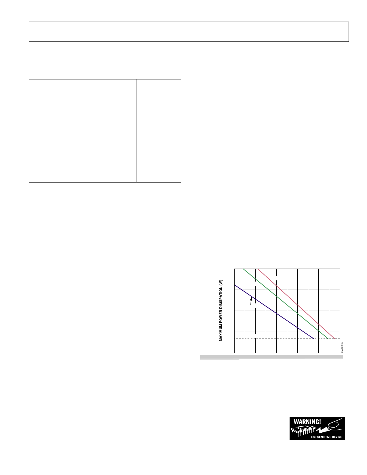
MAXIMUM POWER DISSIPATION
The maximum power that the AD8387 can safely dissipate is
limited by its junction temperature. The maximum safe junction
temperature for plastic encapsulated devices, as determined by the
glass transition temperature of the plastic, is approximately 150°C.
Exceeding this limit temporarily can cause a shift in the parametric
performance due to a change in the stresses exerted on the die by
the package. Exceeding a junction temperature of 150°C for an
extended period can result in device failure.
OPERATING TEMPERATURE RANGE
To ensure operation within the specified operating temperature
range, it is necessary to limit the maximum power dissipation as
follows.
3.0
200LFM
2.5
500LFM
STILL AIR
2.0
1.5
QUIESCENT
THERMAL
SWITCH
ENABLED
DISABLED
1.0
50 55 60 65 70 75 80 85 90 95 100
75 80 85 90 95 100 105 110 115 120 125
AMBIENT TEMPERATURE (°C)
Figure 3. Maximum Power Dissipation vs. Temperature,
AD8387 on a 4-Layer JEDEC PCB with Thermally Optimized Landing
Pattern as Described in the Applications Section
ESD CAUTION
ESD (electrostatic discharge) sensitive device. Electrostatic charges as high as 4000 V readily accumulate on
the human body and test equipment and can discharge without detection. Although this product features
proprietary ESD protection circuitry, permanent damage may occur on devices subjected to high energy
electrostatic discharges. Therefore, proper ESD precautions are recommended to avoid performance
degradation or loss of functionality.
Rev. 0 | Page 5 of 16
Share Link: 