74LVC1G66 Просмотр технического описания (PDF) - NXP Semiconductors.
Номер в каталоге
Компоненты Описание
Список матч
74LVC1G66 Datasheet PDF : 22 Pages
| |||
NXP Semiconductors
74LVC1G66
Bilateral switch
Table 9. Dynamic characteristics …continued
At recommended operating conditions; voltages are referenced to GND (ground = 0 V); for load circuit see Figure 18.
Symbol Parameter
Conditions
−40 °C to +85 °C
−40 °C to +125 °C Unit
Min Typ[1] Max
Min
Max
tdis
disable time
E to Y or Z; see Figure 17
[5]
VCC = 1.65 V to 1.95 V
1.0
4.2
10
1.0
13 ns
VCC = 2.3 V to 2.7 V
1.0
2.4
6.9
1.0
9.0 ns
VCC = 2.7 V
1.0
3.6
7.5
1.0
9.5 ns
VCC = 3.0 V to 3.6 V
1.0
3.4
6.5
1.0
8.5 ns
VCC = 4.5 V to 5.5 V
1.0
2.5
5.0
1.0
6.5 ns
CPD
power dissipation CL = 50 pF; fi = 10 MHz;
[6]
capacitance
VI = GND to VCC
VCC = 2.5 V
VCC = 3.3 V
-
9.8
-
-
- pF
-
12.0
-
-
- pF
VCC = 5.0 V
-
17.3
-
-
- pF
[1] Typical values are measured at Tamb = 25 °C and nominal VCC.
[2] tpd is the same as tPLH and tPHL
[3] propagation delay is the calculated RC time constant of the typical ON resistance of the switch and the specified capacitance when
driven by an ideal voltage source (zero output impedance).
[4] ten is the same as tPZH and tPZL
[5] tdis is the same as tPLZ and tPHZ
[6] CPD is used to determine the dynamic power dissipation (PD in µW).
PD = CPD × VCC2 × fi × N + Σ{(CL + CS(ON))× VCC2 × fo} where:
fi = input frequency in MHz;
fo = output frequency in MHz;
CL = output load capacitance in pF;
CS(ON) = maximum ON-state switch capacitance in pF;
VCC = supply voltage in V;
N = number of inputs switching;
Σ{(CL + CS(ON)) × VCC2 × fo} = sum of the outputs.
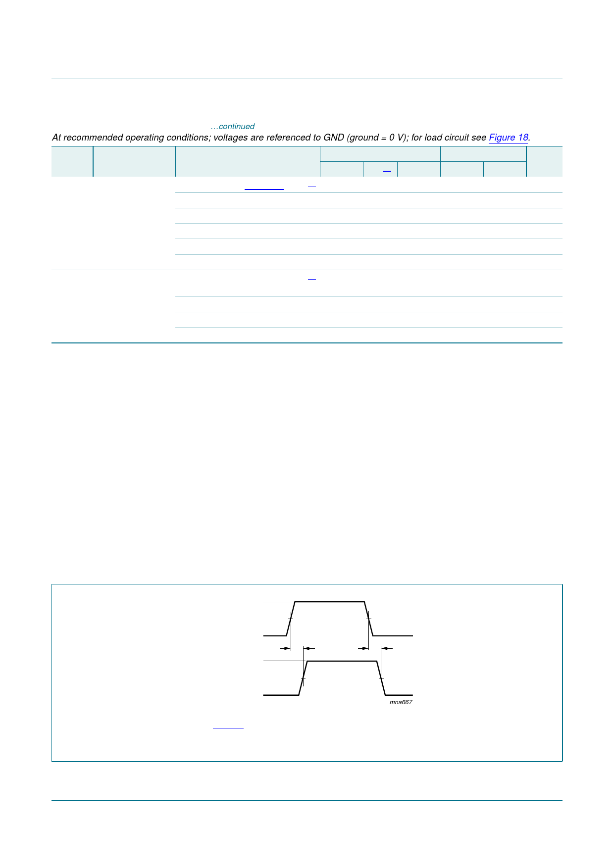
11.1 Waveforms and test circuit
VI
Y or Z input
GND
VOH
Z or Y output
VOL
VM
t PLH
VM
t PHL
mna667
Measurement points are given in Table 10.
Logic levels: VOL and VOH are typical output voltage levels that occur with the output load.
Fig 16. Input (Y or Z) to output (Z or Y) propagation delays
74LVC1G66_6
Product data sheet
Rev. 06 — 27 August 2007
© NXP B.V. 2007. All rights reserved.
10 of 22
Share Link: 