74HC1G66 Просмотр технического описания (PDF) - Philips Electronics
Номер в каталоге
Компоненты Описание
Список матч
74HC1G66 Datasheet PDF : 20 Pages
| |||
Philips Semiconductors
Bilateral switch
Product specification
74HC1G66; 74HCT1G66
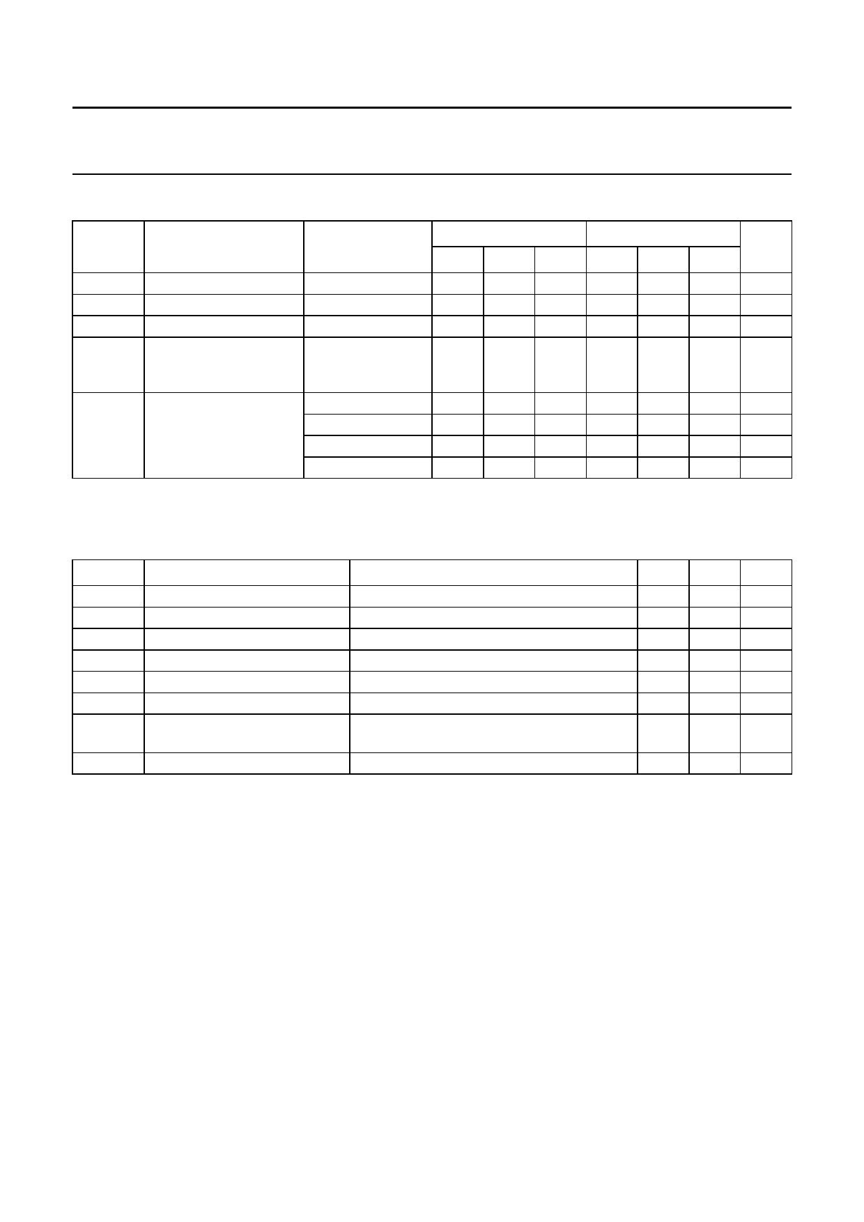
RECOMMENDED OPERATING CONDITIONS
SYMBOL
PARAMETER
VCC
VI
VS
Tamb
supply voltage
input voltage
switch voltage
operating ambient
temperature
tr, tf
input rise and fall times
CONDITIONS
see DC and AC
characteristics per
device
VCC = 2.0 V
VCC = 4.5 V
VCC = 6.0 V
VCC = 10.0 V
74HC1G66
74HCT1G66
UNIT
MIN. TYP. MAX. MIN. TYP. MAX.
2.0 5.0
GND −
GND −
−40 −
10.0 4.5 5.0
VCC GND −
VCC GND −
+125 −40 −
5.5 V
VCC V
VCC V
+125 °C
−
−
1000 −
−
−
ns
−
6.0 500 −
6.0 500 ns
−
−
400 −
−
−
ns
−
−
250 −
−
−
ns
LIMITING VALUES
In accordance with the Absolute Maximum Rating System (IEC 60134); voltages are referenced to GND (ground = 0 V);
see note 1.
SYMBOL
PARAMETER
VCC
supply voltage
IIK
input diode current
ISK
switch diode current
IS
switch source or sink current
ICC
VCC or GND current
Tstg
storage temperature
PD
power dissipation per package
PS
power dissipation per switch
CONDITIONS
VI < − 0.5 V or VI > VCC + 0.5 V
VS < − 0.5 V or VS > VCC + 0.5 V
−0.5 V < VS < VCC + 0.5 V
for temperature range from −40 to + 125 °C;
note 2
MIN.
−0.5
−
−
−
−
−65
−
MAX.
+11.0
±20
±20
±25
±50
+150
200
UNIT
V
mA
mA
mA
mA
°C
mW
−
100 mW
Notes
1. To avoid drawing VCC current out of pin Z, when switch current flows in pin Y, the voltage drop across the
bidirectional switch must not exceed 0.4 V. If the switch current flows into pin Z, no VCC current will flow out of
terminal Y. In this case there is no limit for the voltage drop across the switch, but the voltage at pins Y and Z may
not exceed VCC or GND.
2. Above 55 °C the value of PD derates linearly with 2.5 mW/K.
2002 May 15
4
Share Link: 