74HC1G66 Просмотр технического описания (PDF) - Philips Electronics
Номер в каталоге
Компоненты Описание
Список матч
74HC1G66 Datasheet PDF : 20 Pages
| |||
Philips Semiconductors
Bilateral switch
Product specification
74HC1G66; 74HCT1G66
Type 74HC1G66 and 74HCT1G66
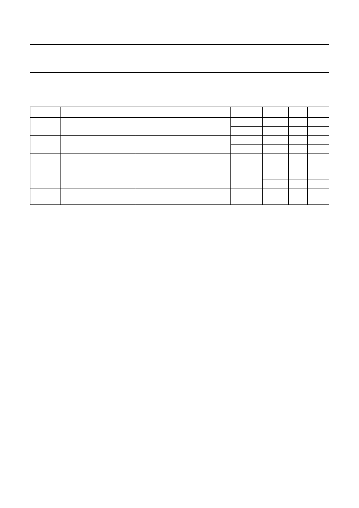
At recommended conditions and typical values. GND = 0 V; tr = tf = 6.0 ns. Vis is the input voltage at pins Y or Z,
whichever is assigned as an input; Vos is the output voltage at pins Y or Z, whichever is assigned as an output.
SYMBOL
PARAMETER
sine-wave distortion
f = 1 kHz
sine-wave distortion
f = 10 kHz
switch OFF signal
feed-through
fmax
minimum frequency
response (−3 dB)
CS
maximum switch
capacitance
TEST CONDITIONS
RL = 10 kΩ; CL = 50 pF; see Fig.12
RL = 10 kΩ; CL = 50 pF; see Fig.12
RL = 600 Ω; CL = 50 pF; f = 1 MHz;
see Figs 9 and 13
RL = 50 Ω; CL = 10 pF;
see Figs 10 and 11
Vis(p-p) (V) VCC (V)
4.0
4.5
8.0
9.0
4.0
4.5
8.0
9.0
note 1
4.5
9.0
note 2
4.5
9.0
TYP.
0.04
0.02
0.12
0.06
−50
−50
180
200
8
UNIT
%
%
%
%
dB
dB
MHz
MHz
pF
Notes
1. Adjust input voltage Vis is 0 dBm level (0 dBM = 1 mW into 600 Ω).
2. Adjust input voltage Vis is 0 dBm level at Vos for 1 MHz (0 dBM = 1 mW into 50 Ω).
2002 May 15
10
Share Link: 