74AHC257 Просмотр технического описания (PDF) - Philips Electronics
Номер в каталоге
Компоненты Описание
Список матч
74AHC257 Datasheet PDF : 20 Pages
| |||
Philips Semiconductors
Quad 2-input multiplexer; 3-state
Product specification
74AHC257;
74AHCT257
FEATURES
• ESD protection:
HBM EIA/JESD22-A114-A exceeds 2000 V
MM EIA/JESD22-A115-A exceeds 200 V
CDM EIA/JESD22-C101 exceeds 1000 V
• Balanced propagation delays
• All inputs have Schmitt-trigger actions
• Non-inverting data path
• Inputs accept voltages higher than VCC
• For AHC only: operates with CMOS input levels
• For AHCT only: operates with TTL input levels
• Specified from −40 to +85 °C and −40 to +125 °C.
DESCRIPTION
The 74AHC/AHCT257 are high-speed Si-gate CMOS
devices and are pin compatible with Low power Schottky
TTL (LSTTL). They are specified in compliance with
JEDEC standard No. 7A.
The 74AHC/AHCT257 has four identical 2-input
multiplexers with 3-state outputs, which select 4 bits of
data from two sources and are controlled by a common
data select input (S).
The data inputs from source 0 (1I0 to 4I0) are selected
when input S is LOW and the data inputs from source 1
(1I1 to 4I1) are selected when S is HIGH. Data appears at
the outputs (1Y to 4Y) in true (non-inverting) form from the
selected inputs.
The 74AHC/AHCT257 is the logic implementation of a
4-pole 2-position switch, where the position of the switch is
determined by the logic levels applied to S. The outputs
are forced to a high impedance OFF-state when OE is
HIGH.
If OE is LOW then the logic equations for the outputs are:
1Y = 1I1 × S + 1I0 × S;
2Y = 2I1 × S + 2I0 × S;
3Y = 3I1 × S + 3I0 × S;
4Y = 4I1 × S + 4I0 × S.
The ‘257’ is identical to the ‘258’ but has non-inverting
(true) outputs.
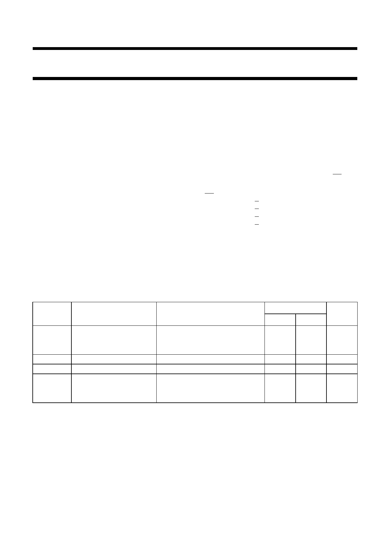
QUICK REFERENCE DATA
GND = 0 V; Tamb = 25 °C; tr = tf ≤ 3.0 ns.
SYMBOL
PARAMETER
tPHL/tPLH
CI
CO
CPD
propagation delay
nl0, nI1 to nY
S to nY
input capacitance
output capacitance
power dissipation
capacitance
CONDITIONS
TYPICAL
AHC AHCT
UNIT
CL = 15 pF; VCC = 5 V
2.9
3.7
ns
CL = 15 pF; VCC = 5 V
3.5
5.1
ns
VI = VCC or GND
3.0
3.0
pF
4.0
4.0
pF
CL = 50 pF; fi = 1 MHz; notes 1 and 2
4 outputs switching via input S
45
51
pF
1 output switching via input I
15
15
pF
Notes
1. CPD is used to determine the dynamic power dissipation (PD in µW).
PD = CPD × VCC2 × fi + ∑ (CL × VCC2 × fo) where:
fi = input frequency in MHz;
fo = output frequency in MHz;
∑ (CL × VCC2 × fo) = sum of outputs;
CL = output load capacitance in pF;
VCC = supply voltage in Volts.
2. The condition is VI = GND to VCC.
2000 Apr 03
2
Share Link: 