74AHC257 Просмотр технического описания (PDF) - Philips Electronics
Номер в каталоге
Компоненты Описание
Список матч
74AHC257 Datasheet PDF : 20 Pages
| |||
Philips Semiconductors
Quad 2-input multiplexer; 3-state
Product specification
74AHC257;
74AHCT257
Type 74AHCT257
GND = 0 V; tr = tf ≤ 3.0 ns.
SYMBOL
PARAMETER
TEST CONDITIONS
WAVEFORMS CL
MIN.
25
TYP.
Tamb (°C)
−40 to +85
MAX. MIN. MAX.
−40 to +125 UNIT
MIN. MAX.
VCC = 4.5 to 5.5 V; note 1
tPHL/tPLH
propagation delay
nI0 to nY; nI1 to nY
propagation delay
S to nY
see Figs 6
and 8
tPZH/tPZL 3-state output enable see Figs 7
time OE to nY
and 8
tPHZ/tPLZ 3-state output disable
time OE to nY
tPHL/tPLH
propagation delay
nI0 to nY; nI1 to nY
propagation delay
S to nY
see Figs 6
and 8
tPZH/tPZL 3-state output enable see Figs 7
time OE to nY
and 8
tPHZ/tPLZ 3-state output disable
time OE to nY
15 pF −
−
−
−
50 pF −
−
−
−
3.7 6.5 1.0 8.0 1.0 9.0 ns
5.1 9.0 1.0 10.5 1.0 11.5 ns
3.9 8.0 1.0 9.0 1.0 10.0 ns
4.5 7.5 1.0 8.0 1.0 8.5 ns
4.9 8.5 1.0 10.0 1.0 11.0 ns
6.4 10.5 1.0 12.5 1.0 13.5 ns
5.1 10.0 1.0 11.0 1.0 12.0 ns
6.5 9.5 1.0 10.5 1.0 11.5 ns
Note
1. Typical values at VCC = 5.0 V.
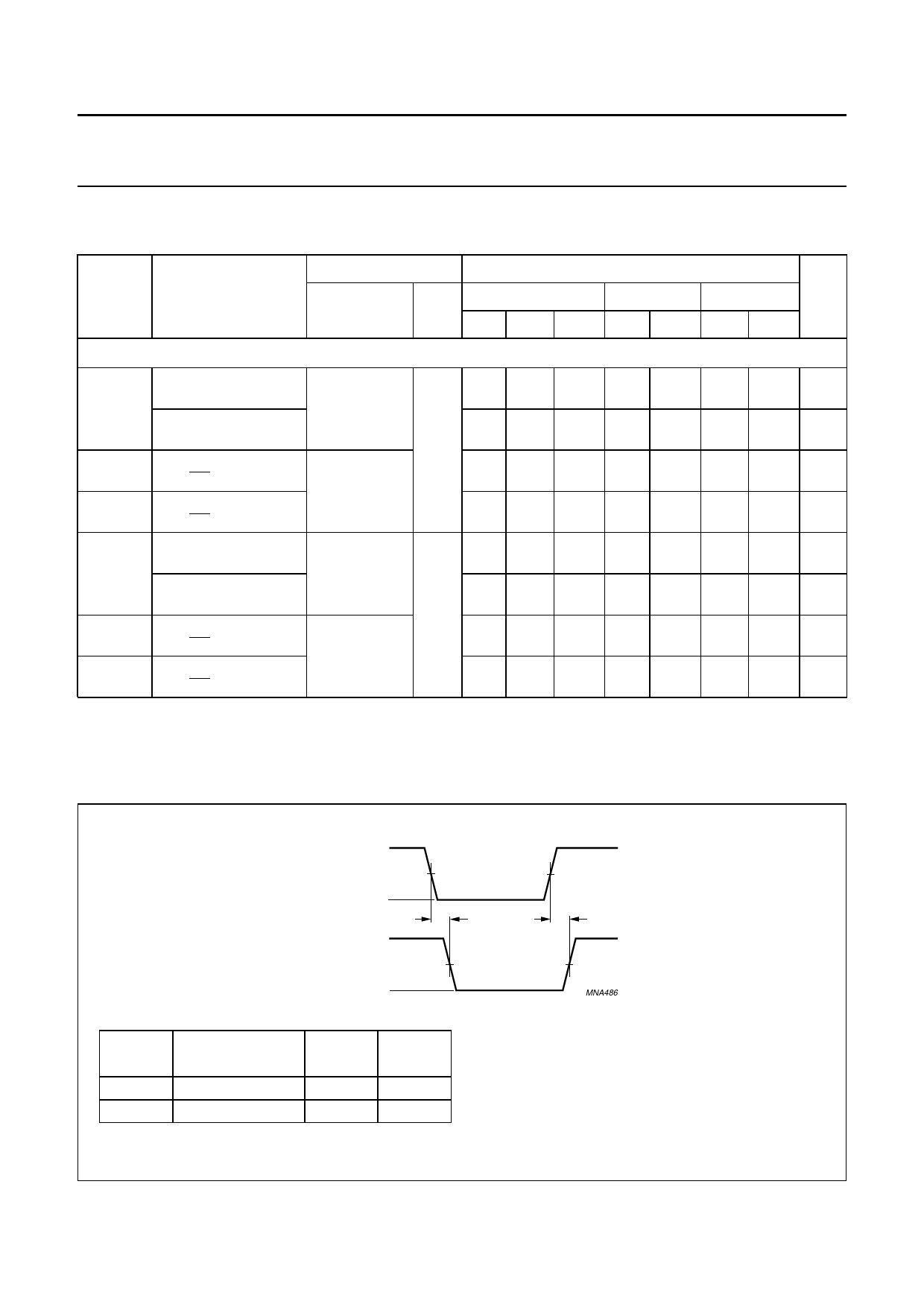
AC WAVEFORMS
handbook, halfpage VI
nI0, nI1, S
input
GND
VOH
nY output
VOL
VM(1)
t PHL
VM(2)
t PLH
MNA486
FAMILY
VI INPUT
REQUIREMENTS
VM(1)
INPUT
VM(2)
OUTPUT
AHC
AHCT
GND to VCC
GND to 3.0 V
50% VCC 50% VCC
1.5 V
50% VCC
Fig.6 The data inputs (1I0, 1I1) and common data select input (S) to output (nY) propagation delays.
2000 Apr 03
10
Share Link: 