74AHC1G32 Просмотр технического описания (PDF) - NXP Semiconductors.
Номер в каталоге
Компоненты Описание
Список матч
74AHC1G32 Datasheet PDF : 12 Pages
| |||
NXP Semiconductors
74AHC1G32; 74AHCT1G32
2-input OR gate
Table 8. Dynamic characteristics …continued
GND = 0 V; tr = tf = ≤ 3.0 ns. For waveform see Figure 5. For test circuit see Figure 6.
Symbol Parameter Conditions
25 °C
−40 °C to +85 °C −40 °C to +125 °C Unit
Min Typ Max Min Max
Min
Max
For type 74AHCT1G32
tpd
propagation A and B to Y;
delay
see Figure 5;
VCC = 4.5 V to 5.5 V
CL = 15 pF
[1]
[3]
-
3.3 6.9 1.0 8.0
1.0
9.0
ns
CL = 50 pF
-
4.8 7.9 1.0 9.0
1.0
10
ns
CPD
power
per buffer;
[4] -
17 -
-
-
-
-
pF
dissipation CL = 50 pF; f = 1 MHz;
capacitance VI = GND to VCC
[1] tpd is the same as tPLH and tPHL.
[2] Typical values are measured at VCC = 3.3 V.
[3] Typical values are measured at VCC = 5.0 V.
[4] CPD is used to determine the dynamic power dissipation PD (µW).
PD = CPD × VCC2 × fi + ∑ (CL × VCC2 × fo) where:
fi = input frequency in MHz;
fo = output frequency in MHz;
CL = output load capacitance in pF;
VCC = supply voltage in Volts.
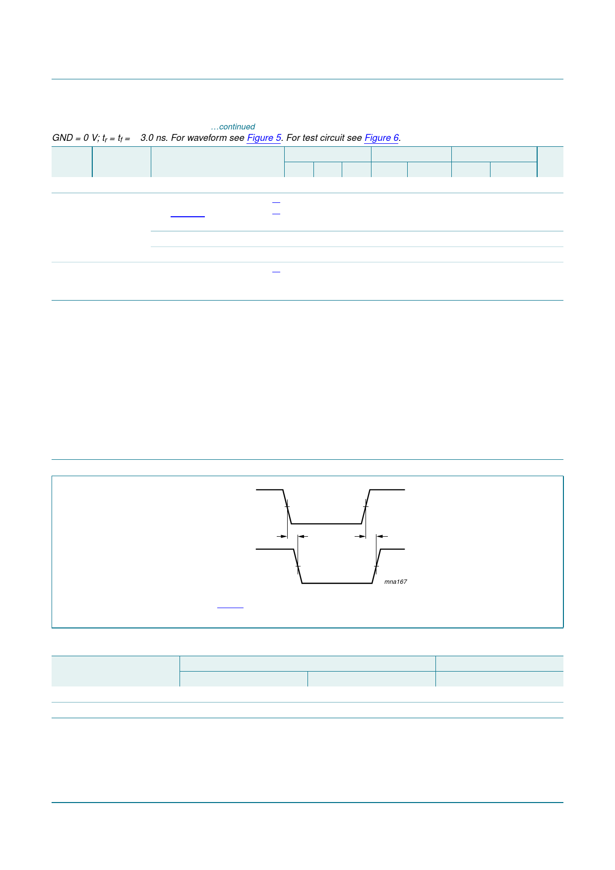
12. Waveforms
A, B input
Y output
VM
tPHL
VM
Measurement points are given in Table 9.
Fig 5. The input (A and B) to output (Y) propagation delays
Table 9. Measurement points
Type number
Input
74AHC1G32
74AHCT1G32
VI
GND to VCC
GND to 3.0 V
VM
0.5 × VCC
1.5 V
tPLH
mna167
Output
VM
0.5 × VCC
0.5 × VCC
74AHC_AHCT1G32_7
Product data sheet
Rev. 07 — 14 May 2009
© NXP B.V. 2009. All rights reserved.
6 of 12
Share Link: 