33710 Просмотр технического описания (PDF) - Freescale Semiconductor
Номер в каталоге
Компоненты Описание
Список матч
33710 Datasheet PDF : 17 Pages
| |||
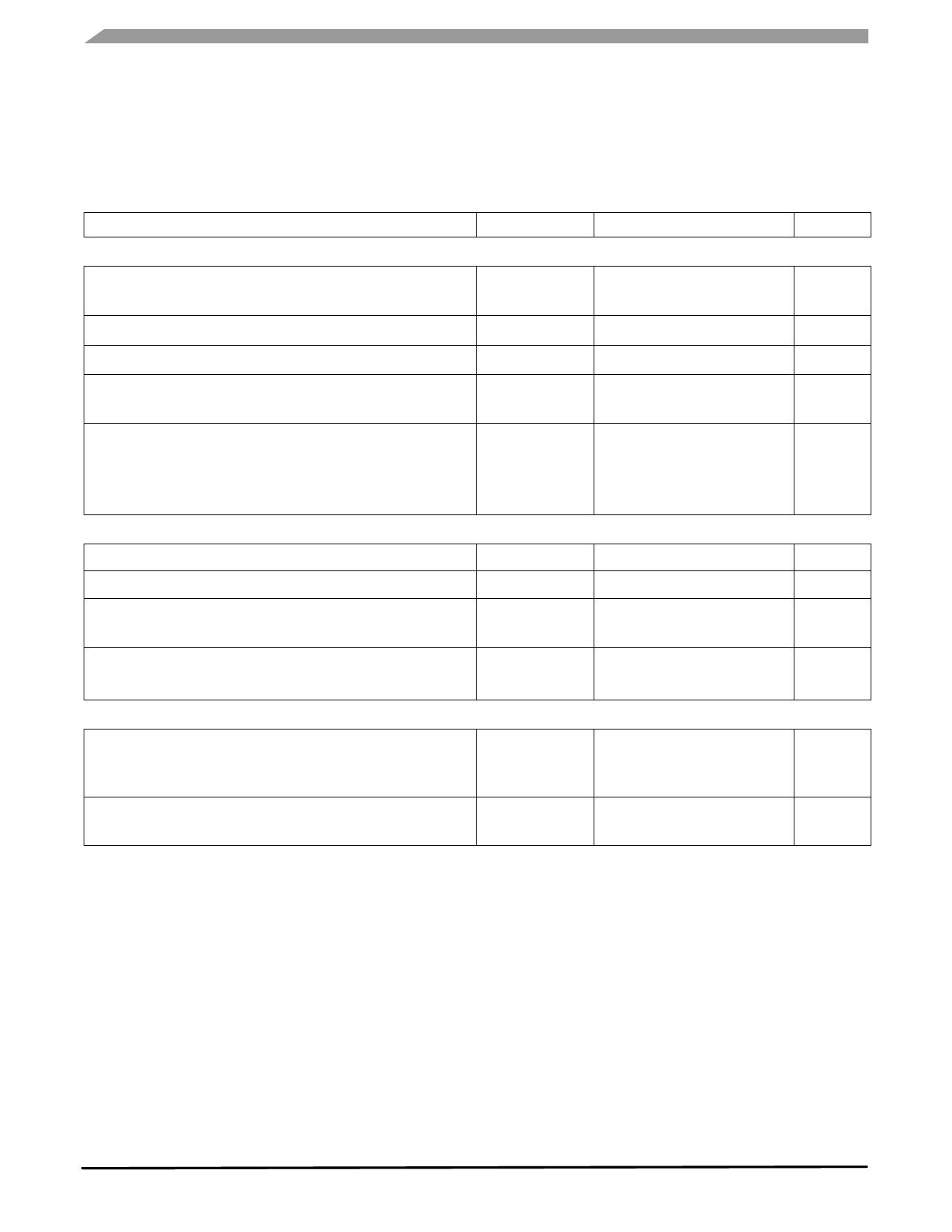
MAXIMUM RATINGS
MAXIMUM RATINGS
MAXIMUM RATINGS
All voltages are with respect to ground unless otherwise noted. Exceeding these ratings may cause a malfunction or permanent
damage to the device.
Rating
Symbol
Max
Unit
ELECTRICAL RATINGS
Input Power Supply Voltage
IB+ = 0.0 A
Terminal Soldering Temperature (1)
Power Dissipation (2)
VB+
V
-0.3 to 36
TSOLDER
260
°C
PD
3.0
W
ESD Standoff Voltage
Non-Operating, Unbiased, Human Body Model (3)
Thermal Resistance
Junction-to-Ambient (4)
Junction-to-Ambient (2)
Junction-to-Exposed-Pad
VESD1
RθJA
RθJA
RθJC
±2000
45
25
2.0
V
°C/W
THERMAL RATINGS
Operating Ambient Temperature
TA
0 to 85
°C
Operating Junction Temperature
TJ
0 to 105
°C
Input Power Supply Voltage
IB+ = 0.0 A to 3.0 A
VB+
V
13 to 32
Quiescent Bias Current from B+ (5)
VB+ = 13 V to 32 V
IB+(Q)
mA
7.5
VI/O SWITCHING REGULATOR (6)
Maximum Output Voltage Startup Overshoot (COUT = 330 µF)
VI / O(STARTUP)
V
Mode0 = 0
5.4
Mode0 = Open
3.6
Maximum Output Current
TA = 0°C to 105°C
IVI/O
mA
700
Notes
1. Soldering temperature limit is for 10 seconds maximum duration. Not designed for immersion soldering. Exceeding these limits may
cause malfunction or permanent damage to the device.
2. With 2.0 in2 of copper heatsink.
3. ESD1 testing is performed in accordance with the Human Body Model (CZAP = 100 pF, RZAP = 1500 Ω).
4. With no additional heatsinking.
5. Maximum quiescent power dissipation is 0.25 W.
6. 13 V ≤ VB+ ≤ 32 V and -20°C ≤ TJ ≤ 145°C unless otherwise noted.
34710
4
Analog Integrated Circuit Device Data
Freescale Semiconductor
Share Link: 