33710 Просмотр технического описания (PDF) - Freescale Semiconductor
Номер в каталоге
Компоненты Описание
Список матч
33710 Datasheet PDF : 17 Pages
| |||
Freescale Semiconductor
Technical Data
Document order number: MC34710
Rev. 3.0, 3/2006
Dual Output DC-DC & Linear
Regulator IC
The 34710 is a dual-output power regulator IC integrating
switching regulator, linear regulator, supervisory and power supply
sequencing circuitry. With a wide operating input voltage range of
13 V to 32 V, the 34710 is applicable to many commercial and
industrial applications using embedded MCUs.
A mode-selected 5.0 V or 3.3 V DC-DC switching regulator is
provided for board-level I/O and user circuitry up to 700 mA. A linear
regulator provides mode-selected core supply voltages of either 3.3V,
2.5V, 1.8V, or 1.5V at currents up to 500 mA.
The supervisor circuitry ensures that the regulator outputs follow a
predetermined power-up and power-down sequence.
Features
• Efficient 5.0 V/3.3 V Buck Regulator
• Low Noise LDO Regulator (mode-selected 3.3V, 2.5V,1.8V, or
1.5V)
• On-Chip Thermal Shutdown Circuitry
• Supervisory Functions (Power-ON Reset and Error Reset
Circuitry)
• Sequenced I/O and Core Voltages
• Pb-Free Packaging Designated by Suffix Code EW
33710
34710
DUAL OUTPUT DC-DC & LINEAR
REGULATOR
DW SUFFIX
EW SUFFIX (PB-FREE)
98ASA10627D
32-TERMINAL SOICW
ORDERING INFORMATION
Device
Temperature
Range (TA)
Package
*PC33710EW / R2
-40°C to 105°
32 SOICW-EP
MC34710EW/R2
0°C to 85°C
32 SOICW-EP
*Device in development.
Electrical parameters being defined.
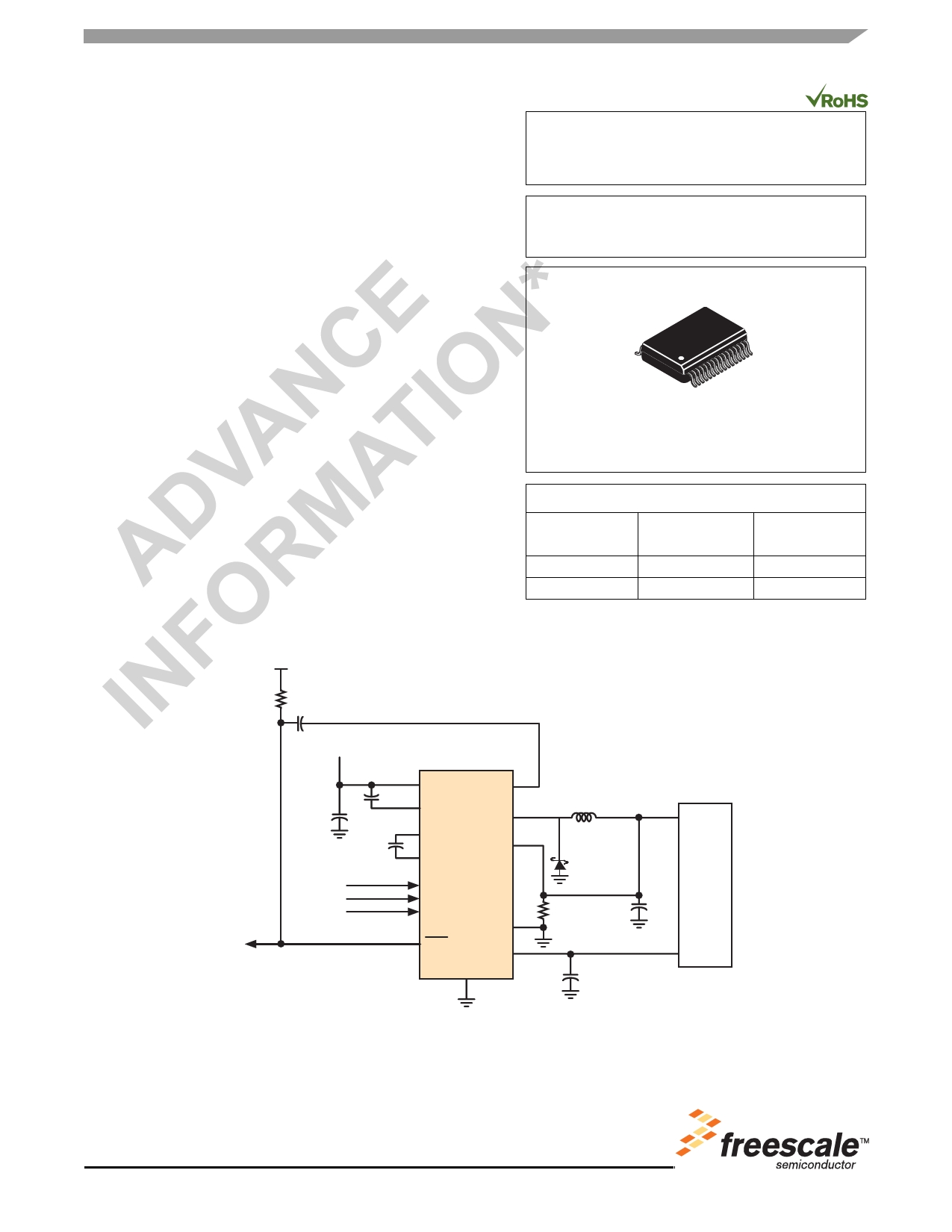
VI/O
13 V to 32 V
34710
B+
CT
VB
VSWITCH
CP2
VFB
CP1
MODE0
MODE1
MODE2
LINB+
RST
VCORE
GND
VI/O
VCORE
MCU
Figure 1. 34710 Simplified Application Diagram
* This document contains certain information on a new product.
Specifications and information herein are subject to change without notice.
© Freescale Semiconductor, Inc., 2006. All rights reserved.
Share Link: 