W83195AR-25 Просмотр технического описания (PDF) - Winbond
Номер в каталоге
Компоненты Описание
Список матч
W83195AR-25 Datasheet PDF : 16 Pages
| |||
W83195AR-25
PRELIMINARY
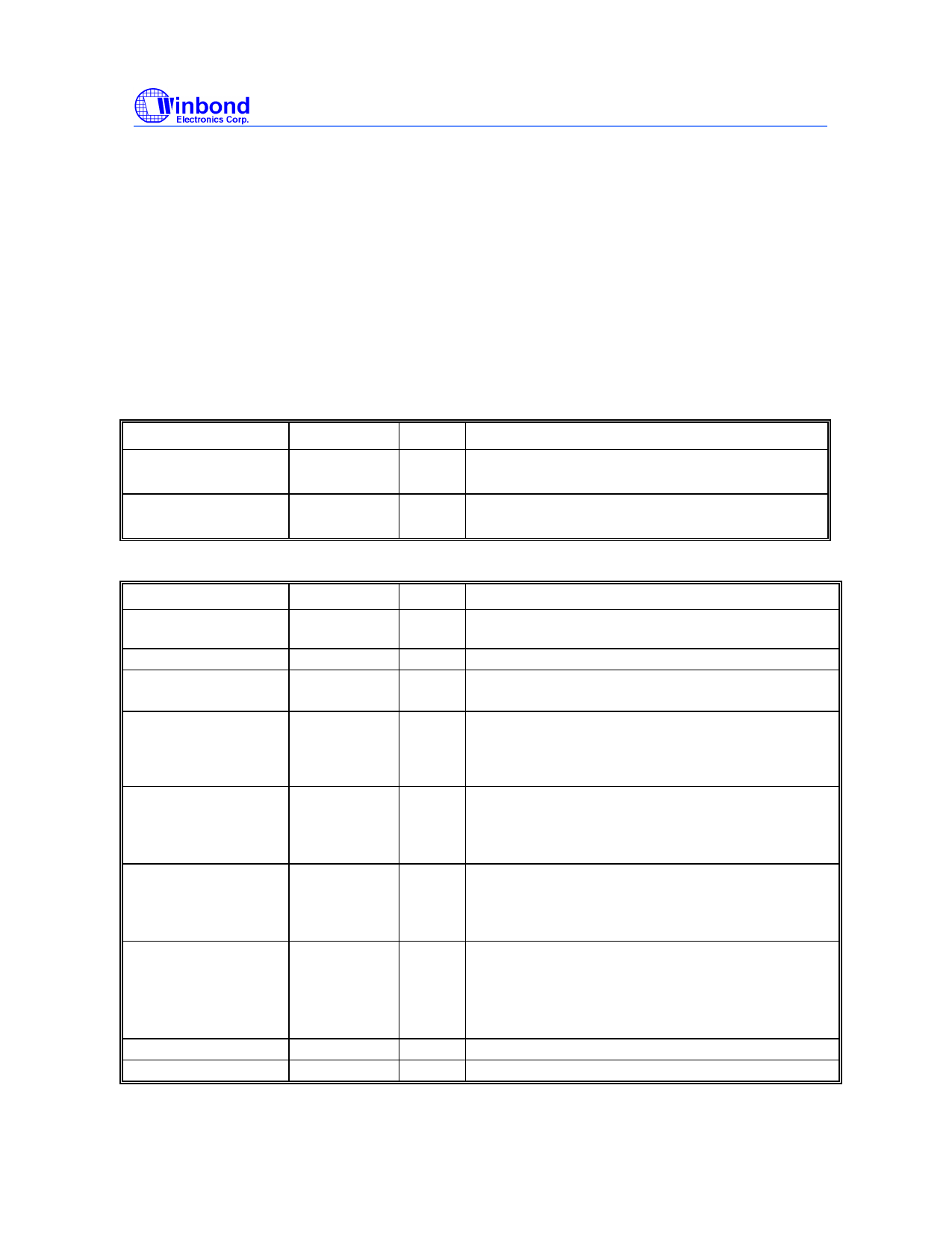
4.0 PIN DESCRIPTION
IN - Input
OUT - Output
I/O - Bi-directional Pin
# - Active Low
* - Internal 250kΩ pull-up
4.1 Crystal I/O
SYMBOL
Xin
Xout
PIN
I/O
FUNCTION
2
IN Crystal input with internal loading capacitors(36pF)
and feedback resistors.
3
OUT Crystal output at 14.318MHz nominally with internal
loading capacitors(36pF).
4.2 CPU, SDRAM, PCI, IOAPIC Clock Outputs
SYMBOL
CPUCLK [0:1]
PD#
IOAPIC
SDRAM_F,
SDRAM[0:11]
PCICLK0/ *FS0
PIN
52,51
22
54
38, 48,47,46,
44,43,42,40,
39,31, 30,27,
26
11
PCICLK1/ FS1#
12
PCICLK2/ *SEL24_48
12
I/O
OUT
IN
OUT
OUT
FUNCTION
Low skew (< 250ps) clock outputs for host
frequencies such as CPU and Chipset.
Power Down mode when driven low.
Clock outputs synchronous with PCI clock and
powered by VddA.
SDRAM clock outputs.
I/O 3.3V 33MHz PCI clock during normal operation.
Latched input for FS0 at initial power up for H/W
selecting the output frequency of CPU, SDRAM and
PCI clocks(Default=1).
I/O Low skew (< 250ps) PCI clock outputs.
Latched input for FS1 at initial power up for H/W
selecting the output frequency of CPU, SDRAM and
PCI clocks(Default=0).
I/O Low skew (< 250ps) PCI clock outputs.
Latched input for SEL24_48 at initial power up for the
output frequency of 24MHz(HIGH) and 48MHz(LOW)
clocks.
PCICLK [ 3:7 ]
3V66 [0:2]
15,16,17,19,20 OUT Low skew (< 250ps) PCI clock outputs.
6,7,8
OUT 3.3V output clocks for the chipset.
Publication Release Date: Jan. 2000
-3-
Revision 0.40
Share Link: 