LV23200T Просмотр технического описания (PDF) - SANYO -> Panasonic
Номер в каталоге
Компоненты Описание
Список матч
LV23200T Datasheet PDF : 17 Pages
| |||
LV23200T
Continued from preceding page.
No. Control block data
Description
(6)
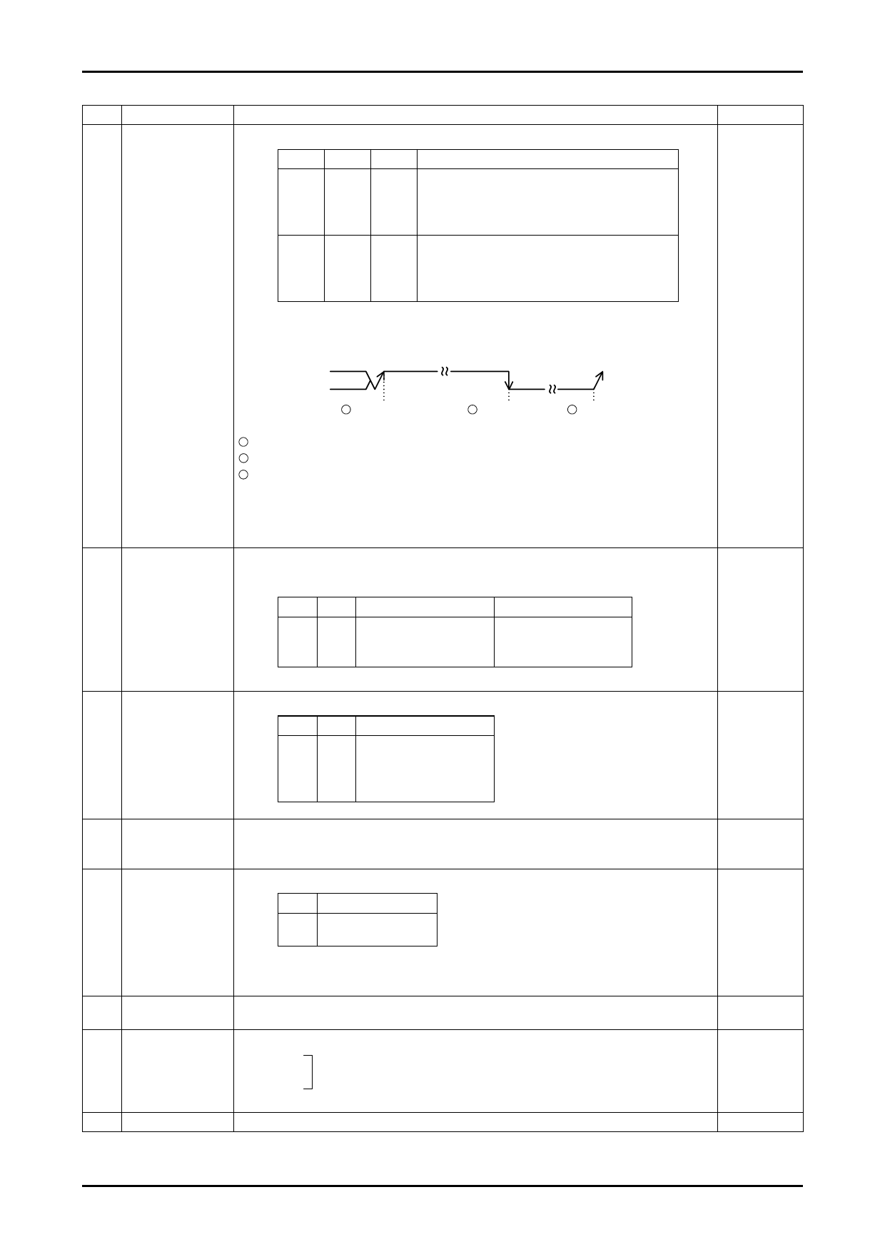
DO pin
• Data to control DO pin output
control data
DOC2 DOC1 DOC0
DO pin condition
DOC0
DOC1
DOC2
0
0
0
Open
0
0
1
Low when unlock is detected.
0
1
0
end-UC (See the item with asterisk below)
0
1
1
Open
1
0
0
Open
1
0
1
Low when SDON
1
1
0
Low when stereo
1
1
1
Open
• The open condition is selected at power ON/reset.
* IF counter counting end check
Related data
UL0, UL1
CTE
DO pin
1 Counting start
2 Counting end 3 CE : HI
1 With end-UC set and IF counter starting (CTE = 0→1), DO pin opens automatically.
2 At end of counting of the IF counter, DO pin goes LOW and check on counting end can be made.
3 DO pin opens when serial data is entered/output (CE pin : Hi)
Note : DO pin is always in the open condition during data input (IN1 and IN2 modes, during CE : Hi
period), regardless of DO pin control data (DOC0 to 2). In the DO pin condition during data output
(OUT mode, CE-Hi period), the content of internal DO serial data is output in synchronization with
CL pin signal, regardless of DO pin control data (DOC).
(7)
Unlock detection
• Phase error (φE) detection width selection data to judge if PLL is locked.
data
Phase error exceeding the detection width is judged to mean that PLL is locked
(* : don’t care)
UL0, UL1
UL1 UL0
φE Detection width
Detection output
0
0
Stop
Open
0
1
1
*
0
±6.67µs
Direct output of φE
φE extended by 1 to 2 ms
DOC0
DOC1
DOC2
* DO pin is LOW. Serial data output : UL = 0.
(8)
Phase
• Data to control the dead zone of phase comparator
comparator
control data
DZ1 DZ0
0
0
Dead zone mode
DZA
DZ0, DZ1
0
1
1
0
DZB
DZC
1
1
DZD
Dead zone width : DZA<DZB<DZC<DZD
(9)
Output port data
• Data to determine the output of output ports BO1 and BO2
“Data” = 0 : OPEN
BO
1 : Low
(10)
Charge pump
• Data to enforce control of charge pump output
control data
DLC Charge pump output
DLC
0
Normal
1
Forced to LOW
* In case of dead lock because of VCO oscillation stop when the VCO control voltage (Vtune) is 0V, it
is possible to clear dead lock by setting the charge pump output to LOW and V tune to VCC. (Dead
lock clear circuit)
(11)
IFS
• Normally, set Data = 1. Setting Data = 0 causes the input sensitivity worsening mode and the
sensitivity decreases by about 10 to 30mVrms.
(12)
LSI test data
• LSI test data
TEST0
TEST0 to 2
TEST1
All to be set to “0”
TEST2
All set to zero at power ON/reset
(13)
DNC
• Set data = 0.
Continued on next page.
No.8301-11/17
Share Link: 