V826516G04SXTG-B0 Просмотр технического описания (PDF) - Mosel Vitelic, Corp
Номер в каталоге
Компоненты Описание
Список матч
V826516G04SXTG-B0 Datasheet PDF : 14 Pages
| |||
MOSEL VITELIC
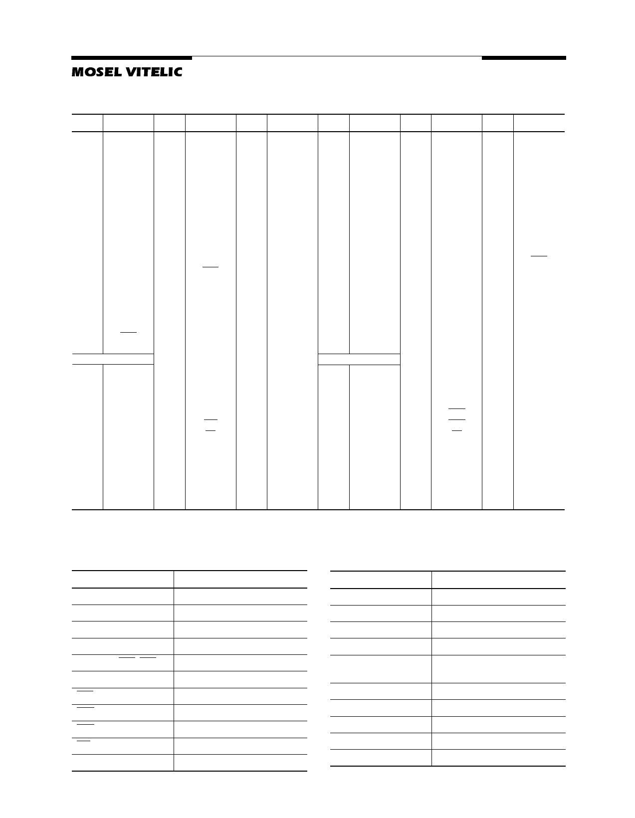
Pin Configurations (Front Side/Back Side)
Pin
Front
1
VREF
3
VSS
5
DQ0
7
DQ1
9
VDD
11
DQS0
13
DQ2
15
VSS
17
DQ3
19
DQ8
21
VDD
23
DQ9
25
DQS1
27
VSS
29
DQ10
31
DQ11
33
VDD
35
CK0
37
CK0
39
VSS
Key
41
DQ16
43
DQ17
45
VDD
47
DQS2
49
DQ18
51
VSS
53
DQ19
55
DQ24
57
VDD
59
DQ25
61
DQS3
63
VSS
65
DQ26
Pin
Front
Pin
Front
67
DQ27
135
DQ34
69
VDD
137
VSS
71
CB0
139
DQ35
73
CB1
141
DQ40
75
VSS
143
VDD
77
DQS8
145
DQ41
79
CB2
147
DQS5
81
VDD
149
VSS
83
CB3
151
DQ42
85
DU
153
DQ43
87
VSS
155
VDD
89
CK2
157
VDD
91
CK2
159
VSS
93
VDD
161
VSS
95
CKE1
163
DQ48
97 DU(A13) 165
DQ49
99
A12
167
VDD
101
A9
169
DQS6
103
VSS
171
DQ50
105
A7
173
VSS
107
A5
175
DQ51
109
A3
177
DQ56
111
A1
179
VDD
113
VDD
181
DQ57
115 A10/AP 183
DQS7
117
BA0
185
DQ58
119
WE
187
DQ58
121
S0
189
DQ59
123
DU
191
VDD
125
VSS
193
SDA
127
DQ32
195
SCL
129
DQ33
197 VDDSPD
131
VDD
199
VDDID
133
DQS4
Pin
Back
2
VREF
4
VSS
6
DQ4
8
DQ5
10
VDD
12
DM0
14
DQ6
16
VSS
18
DQ7
20
DQ12
22
VDD
24
DQ13
26
DM1
28
VSS
30
DQ14
32
DQ15
34
VDD
36
VDD
38
VSS
40
VSS
Key
42
DQ20
44
DQ21
46
VDD
48
DM2
50
DQ22
52
VSS
54
DQ23
56
DQ28
58
VDD
60
DQ29
62
DM3
64
VSS
66
DQ30
Notes:
* These pins are not used in this module.
Pin Names
Pin
A0~A11
BA0~BA1
DQ0~DQ63
DQS0~DQS7
CK0~CK2, CK0~CK2,
CKE0
CS0
RAS
CAS
WE
DM0~DM7
Pin Description
Address Input (Multiplexed)
Bank Select Address
Data Input/Output
Data Strobe Input/Output
Clock Input
Clock Enable Input
Chip Select Input
Row Address Strobe
Column Address Strobe
Write Enable
Data - In Mask
Pin
VDD
VDDQ
VSS
VREF
VDDSPD
SDA
SCL
SA0~2
VDDID
NC
V826516G04S Rev. 1.5 March 2002
4
V826516G04S
Pin
Back
Pin
68
DQ31
136
70
VDD
138
72
CB4
140
74
CB5
142
76
VSS
144
78
DM8
146
80
CB6
148
82
VDD
150
84
CB7
152
86 DU/(RESET) 154
88
VSS
156
90
VSS
158
92
VDD
160
94
VDD
162
96
CKE0
164
98 DU(BA2) 166
100
A11
168
102
A8
170
104
VSS
172
106
A6
174
108
A4
176
110
A2
178
112
A0
180
114
VDD
182
116
BA1
184
118
RAS
186
120
CAS
188
122
S1
190
124
DU
192
126
VSS
194
128
DQ36
196
130
DQ37
198
132
VDD
200
134
DM4
Back
DQ38
VSS
DQ39
DQ44
VDD
DQ45
DM5
VSS
DQ46
DQ47
VDD
CK1
CK1
VSS
DQ52
DQ53
VDD
DM6
DQ54
VSS
DQ55
DQ60
VDD
DQ61
DM7
VSS
DQ62
DQ63
VDD
SA0
SA1
SA2
DU
Pin Description
Power Supply (2.5V)
Power Supply for DQS(2.5V)
Ground
Power Supply for Reference
Serial EEPOM Power Supply (2.3V
to 3.6V)
Serial Data I/O
Serial Clock
Address in EEPROM
VDD Identification Flag
No Connection
Share Link: 