UL631H256 Просмотр технического описания (PDF) - Unspecified
Номер в каталоге
Компоненты Описание
Список матч
UL631H256 Datasheet PDF : 12 Pages
| |||
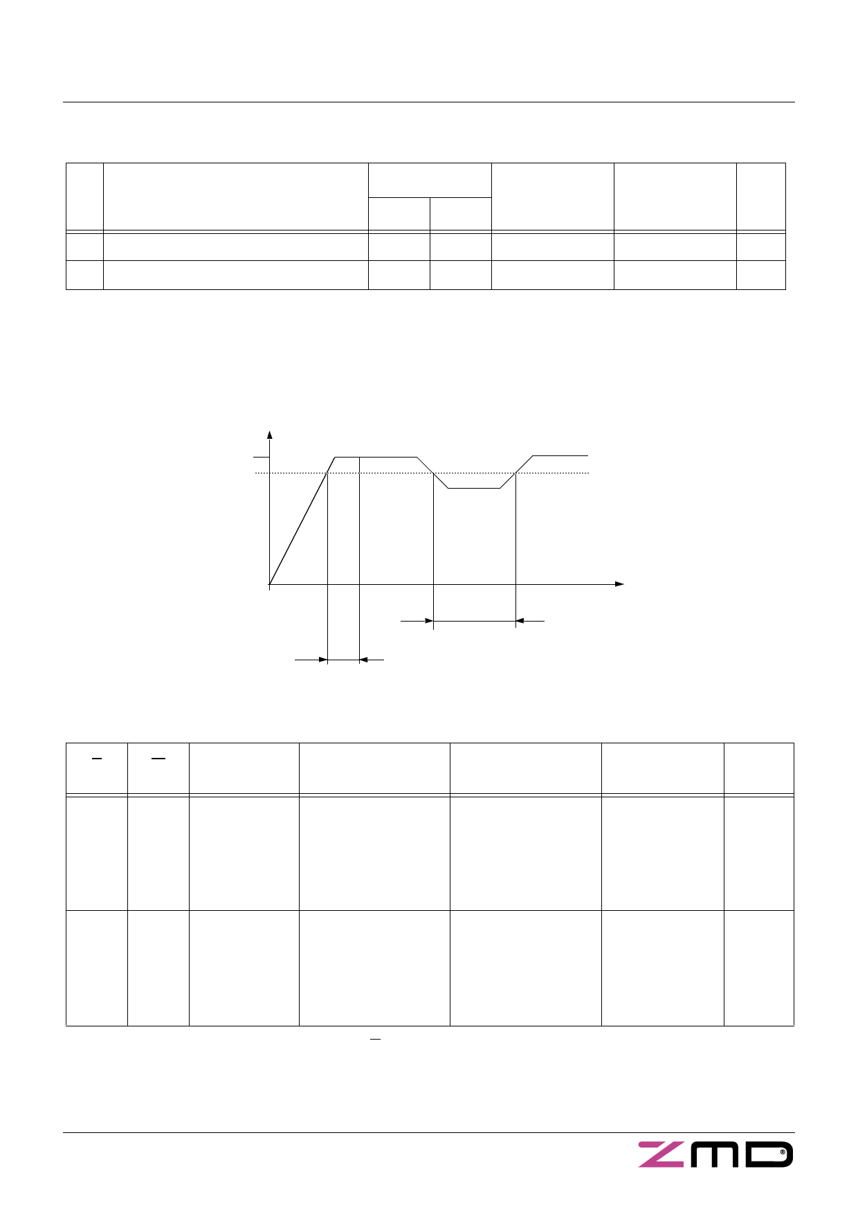
Nonvolatile Memory Operations
No.
STORE Cycle Inhibit and
Automatic Power Up RECALL
Symbol
Alt.
IEC
24 Power Up RECALL Durationk
Low Voltage Trigger Level
tRESTORE
VSWITCH
k: tRESTORE starts from the time VCC rises above VSWITCH.
STORE Cycle Inhibit and Automatic Power Up RECALL
VCC
3.0 V
VSWITCH
Min.
2.4
UL631H256
Max.
Unit
650
µs
2.7
V
Power Up
RECALL
Software Mode Selection
(24)
tRESTORE
t
STORE inhibit
E
W
A13 - A0
(hex)
Mode
I/O
L
H
0E38
31C7
03E0
3C1F
303F
0FC0
Read SRAM
Read SRAM
Read SRAM
Read SRAM
Read SRAM
Nonvolatile STORE
Output Data
Output Data
Output Data
Output Data
Output Data
Output High Z
L
H
0E38
31C7
03E0
3C1F
303F
0C63
Read SRAM
Read SRAM
Read SRAM
Read SRAM
Read SRAM
Nonvolatile RECALL
Output Data
Output Data
Output Data
Output Data
Output Data
Output High Z
Power
Active
ICC2
Active
Notes
l, m
l, m
l, m
l, m
l, m
l, m
l, m
l, m
l, m
l, m
l, m
l, m
l: The six consecutive addresses must be in order listed. W must be high during all six consecutive cycles. See STORE cycle and RECALL
cycle tables and diagrams for further details.
The following six-address sequence is used for testing purposes and should not be used: 0E38, 31C7, 03E0, 3C1F, 303F, 339C.
m: While there are 15 addresses on the UL631H256, only the lower 14 are used to control software modes.
April 7, 2005
7
Share Link: 