UL631H256 Просмотр технического описания (PDF) - Unspecified
Номер в каталоге
Компоненты Описание
Список матч
UL631H256 Datasheet PDF : 12 Pages
| |||
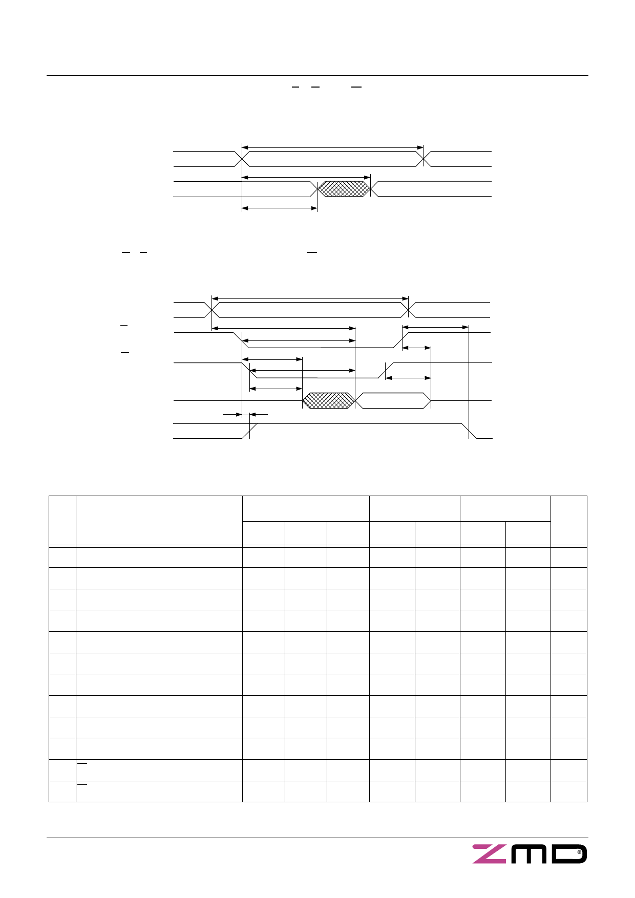
Read Cycle 1: Ai-controlled (during Read cycle: E = G = VIL, W = VIH)f
UL631H256
Ai
DQi
Output
tcR (1)
Address Valid
ta(A) (2)
Previous Data Valid
tv(A) (9)
Output Data Valid
Read Cycle 2: G-, E-controlled (during Read cycle: W = VIH)g
Ai
E
G
DQi
Output
ICC
tcR (1)
Address Valid
ta(A) (2)
ta(E) (3)
ten(E) (7)
ta(G) (4)
High Impedance
ten(G) (8)
ACTIVE
tPU (10)
STANDBY
tPD (11)
tdis(E) (5)
tdis(G) (6)
Output Data Valid
No.
Switching Characteristics
Write Cycle
Symbol
Alt. #1 Alt. #2 IEC
35
Min.
Max.
12 Write Cycle Time
tAVAV
tAVAV
tcW
35
13 Write Pulse Width
tWLWH
tw(W)
25
14 Write Pulse Width Setup Time
tWLEH tsu(W)
25
15 Address Setup Time
tAVWL
tAVEL
tsu(A)
0
16 Address Valid to End of Write
tAVWH tAVEH tsu(A-WH)
25
17 Chip Enable Setup Time
tELWH
tsu(E)
25
18 Chip Enable to End of Write
tELEH
tw(E)
25
19 Data Setup Time to End of Write tDVWH tDVEH tsu(D)
12
20 Data Hold Time after End of Write tWHDX tEHDX th(D)
0
21 Address Hold after End of Write
tWHAX tEHAX
th(A)
0
22 W LOW to Output in High-Zh, i
tWLQZ
tdis(W)
13
23 W HIGH to Output in Low-Z
tWHQX
ten(W)
5
45
Unit
Min.
Max.
45
ns
30
ns
30
ns
0
ns
30
ns
30
ns
30
ns
15
ns
0
ns
0
ns
15
ns
5
ns
April 7, 2005
5
Share Link: 