CS5511(2000) Просмотр технического описания (PDF) - Cirrus Logic
Номер в каталоге
Компоненты Описание
Список матч
CS5511 Datasheet PDF : 26 Pages
| |||
CS5510/11/12/13
2.5 Performing Conversions
After power and a clock source are established to
the CS5510/11/12/13, the ADCs begin performing
conversions. The three sections that follow explain
how to read conversion data from each ADC, and
decode the conversion word into the respective flag
and data bits. Keep in mind that in the CS5510/12,
SCLK provides the external clock source for the
converter. Data is clocked from the CS5510/12 at
the rate set by the external clock source (typically
32.768 kHz). The CS5511/13 provides an on-chip
oscillator for the master clock. In the CS5511/13,
SCLK is asynchronous to the on-chip oscillator and
can be clocked at a rate up to 2 MHz.
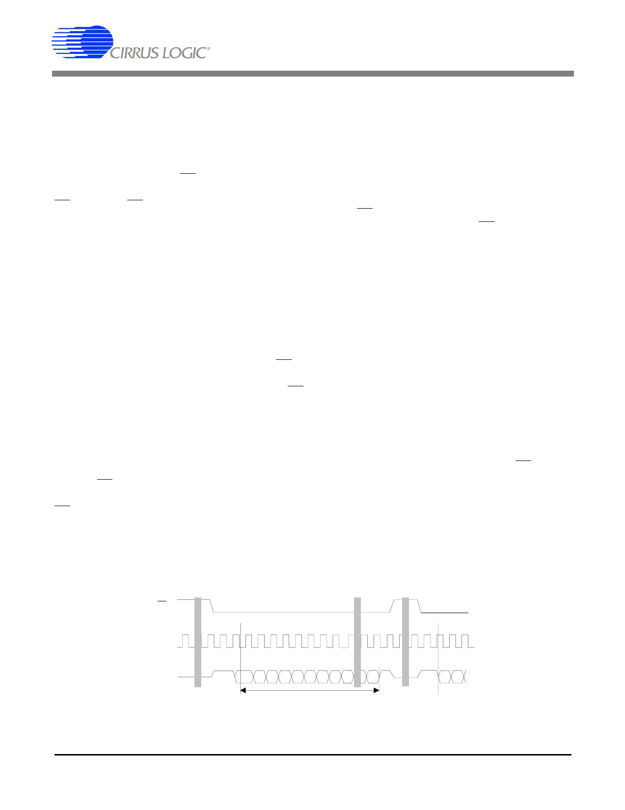
2.5.1 Reading Conversions - CS5510/12
After power-up, the CS5510/12 will begin convert-
ing once a clock source is applied to the SCLK pin.
When a conversion has completed, and there is new
data in the output register, the SDO line will fall to
a logic low level if CS is also at a logic low state
(SDO will always be high-impedance when CS is
high). If CS is low at the end of the conversion cy-
cle, SDO will fall on the rising edge of an SCLK.
After SCLK falls, the next SCLK cycle (high, then
low) will begin clocking out the data. The first
data bit therefore, is 1 and 1/2 SCLK cycles wide.
Twenty-four SCLK cycles (after the initial high-
low transition) are needed to retrieve the conver-
sion word from the part (see Figures 16 and 17).
The data bits can be read on the rising edge of
SCLK, and the next data bit is output to SDO on the
falling edge of SCLK. Once the entire data word
has been read, SDO will return to a logic high state
until there is a new conversion word available. If
CS is at a logic high at the end of the conversion cy-
cle, the data will not be shifted out of the part until
CS is brought to a logic low state during the next
conversion cycle. If a new conversion becomes
available while the current data is being read, the
data register will not be updated, and the new con-
version word will be lost. The user need not read
every conversion. If the user chooses not to read a
conversion, CS should remain at a logic high state
for the duration of the conversion cycle. Note that
if CS goes to a logic high state during a read, the
current conversion data will be lost and replaced by
a new conversion word when the new conversion
data is available.
2.5.2 Reading Conversions - CS5511/13
After power-up, the CS5511/13 begins converting
and updating the output register. When there is new
data in the output register (at the end of a conver-
sion cycle) the SDO line will fall to a logic low lev-
el if CS is also at a logic low state (SDO will always
be high-impedance when CS is high). Twenty-four
SCLK cycles are needed to retrieve the conversion
word from the part (see Figures 18 and 19). The
data bits can be read on the rising edge of SCLK,
and the next data bit is output to SDO on the falling
edge of SCLK. Once the entire data word has been
read, SDO will return to a logic high state until
there is a new conversion word available. If new
conversions become available while the current
data is being read, the data register will not be up-
dated, and the new conversions will be lost. The
user need not read every conversion. If the user
chooses not to read a conversion after SDO falls,
SDO will rise seventeen oscillator clock cycles (of
the internal oscillator) before the next conversion
word is available and then fall again to signal that
the conversion is complete. Note that if a conver-
sion word is not read before the next conversion
word is ready, or if CS goes to a logic high state
during a read, the current conversion data will be
lost and replaced by a new conversion word when
the new conversion data is available.
16
DS337F1
Share Link: 