CS5511(2000) Просмотр технического описания (PDF) - Cirrus Logic
Номер в каталоге
Компоненты Описание
Список матч
CS5511 Datasheet PDF : 26 Pages
| |||
CS5510/11/12/13
2.3.1 Digital Logic Levels
The many power supply configurations available in
the CS5510/11/12/13 allow for a wide range of dig-
ital logic levels. The logic high input and output
levels are determined by the V+ pin. The logic low
output on SDO is referenced to and driven by the
current logic-low voltage on CS. Since the
CS5510/11/12/13 do not include a dedicated
ground pin, CSLow defines the logic low level for
the digital interface. Figures 9 and 10 illustrate the
threshold levels of the CS5510/11/12/13 serial in-
terface (CS, SCLK, and SDO).
To accommodate opto-isolators, the SCLK input is
designed with a Schmitt-trigger to allow an opto-
isolator with slower rise and fall times to directly
drive the pin. Additionally, SDO is capable of sink-
ing up to 1 mA or sourcing up to 5 mA to directly
drive an opto-isolator LED. SDO will have less
than a 600 mV loss in the drive voltage when sink-
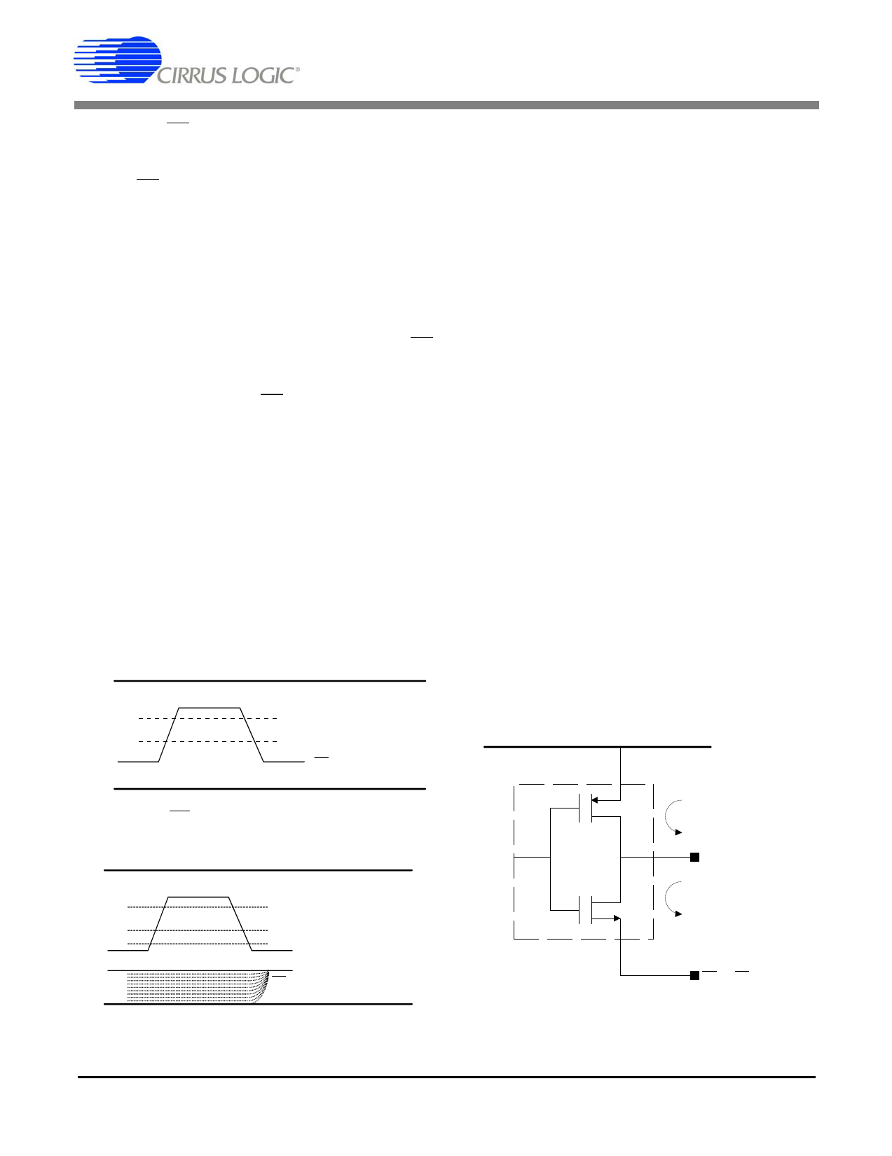
ing or sourcing its current. As shown in Figure 11,
the CS signal provides the sink current path for the
SDO pin when its voltage is low (i.e. the voltage
specified for SDO is relative to CSLow.).
V+
2.4 Clock Generator
The CS5510/12 and CS5511/13 provide distinct
modes for generating the master clock for the
ADCs. The CS5510/12 uses the SCLK input pin as
its operating clock. The CS5511/13 has an on-chip
oscillator that provides its master clock. The SCLK
pin on the CS5511/13 is used only to read data and
to put the part into sleep mode.
2.4.1 External Clock Source for
CS5510/12
The user must provide an external (CMOS compat-
ible) clock to the CS5510/12. The clock is input to
SCLK where it is then divided down to provide the
master clock for the ADC. The output word rate
(OWR) for the CS5510/12 is derived from the
SCLK, and is equal to SCLK/612. Figure 12 illus-
trates an external 32.768 kHz (CMOS compatible)
clock oscillator that a user might consider.
Another clock generation option is to use a micro-
controller. Some microcontrollers have dedicated
timer/counter circuitry which can generate a clock
signal on an output pin with no software overhead.
Such a microcontroller circuit is shown in
Figure 13.
VIH == V+ - 0.45V
VIL = 0.5 (V+ - V-) + 0.6V + V-
CS LOW
V-
Figure 9. CS and SCLK Digital Input Levels.
V+
Output Drive Logic
5 mA Max Source
V+
VOH= V+ - 0.6V
VOL = CS LOW + 0.6V
VIL
CS LOW
V-
Figure 10. SDO Digital Output Levels.
SDO (from SDO
Control Logic)
1 mA Max Sink
CS (to CS
Control Logic)
Figure 11. Serial Port Output Drive Logic.
14
DS337F1
Share Link: 