CS5525-BS Просмотр технического описания (PDF) - Cirrus Logic
Номер в каталоге
Компоненты Описание
Список матч
CS5525-BS Datasheet PDF : 29 Pages
| |||
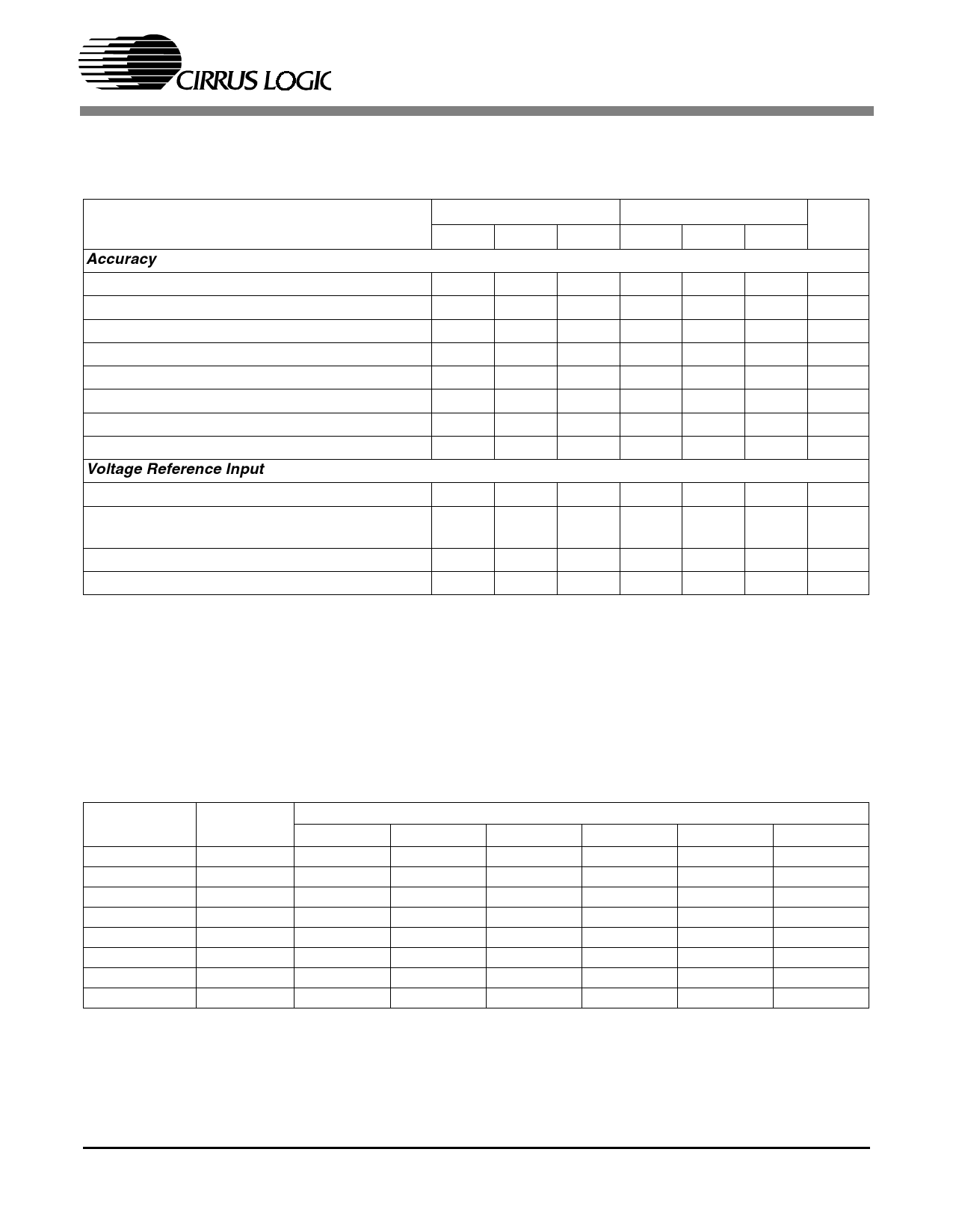
CS5525 CS5526
ANALOG CHARACTERISTICS (TA = 25 °C; VA+, VD+ = 5 V ±5%; VREF+ = 2.5 V, VREF- = AGND,
NBV = -2.1 V, FCLK = 32.768 kHz, OWR (Output Word Rate) = 15 Hz, Bipolar Mode, Input Range = ±100 mV;
See Notes 1 and 2.)
CS5525
CS5526
Parameter
Min Typ Max
Accuracy
Linearity Error
- ±0.0015 ±0.003
No Missing Codes
16
-
-
Bipolar Offset
(Note 3) -
±1
±2
Unipolar Offset
(Note 3) -
±2
±4
Offset Drift
(Notes 3 and 4) -
20
-
Bipolar Gain Error
-
±8
±31
Unipolar Gain Error
-
±16 ±62
Gain Drift
(Note 4) -
1
3
Voltage Reference Input
Range
(VREF+) - (VREF-)
1
2.5
3.0
Common Mode Rejection dc
50, 60 Hz
-
110
-
-
130
-
Input Capacitance
-
16
-
CVF Current
(Note 5) -
0.6
-
Min Typ Max Unit
- ±0.0007 ±0.0015 %FS
20
-
-
Bits
-
±16 ±32 LSB
-
±32 ±64 LSB
-
20
-
nV/°C
-
±8
±31 ppm
-
±16 ±62 ppm
-
1
3 ppm/°C
1
2.5
3.0
V
-
110
-
dB
-
130
-
dB
-
16
-
pF
-
0.6
-
µA/V
Notes: 1. Applies after system calibration at any temperature within -40 °C ~ +85 °C.
2. Specifications guaranteed by design, characterization, and/or test.
3. Specification applies to the device only and does not include any effects by external parasitic
thermocouples. LSB = LSB16 for the CS5525, and LSB20 for the CS5526.
4. Drift over specified temperature range after calibration at power-up at 25 °C.
5. See the section of the data sheet which discusses input models on page 15.
RMS NOISE (Notes 6 and 7)
Output Rate
(Hz)
3.76
7.51
15.0
30.1
60.0
123.2 (Note 8)
168.9 (Note 8)
202.3 (Note 8)
-3 dB Filter
Frequency
3.27
6.55
12.7
25.4
50.4
103.6
141.3
169.2
25 mV
90 nV
110 nV
170 nV
250 nV
500 nV
2.0 µV
10 µV
30 µV
Input Range, (Bipolar/Unipolar Mode)
55 mV
100 mV
1V
2.5 V
90 nV
130 nV
1.0 µV
2.0 µV
130 nV
190 nV
1.5 µV
3.0 µV
200 nV
250 nV
2.0 µV
5.0 µV
300 nV
500 nV
4.0 µV
10 µV
1.0 µV
1.5 µV
15 µV
45 µV
4.0 µV
8.0 µV
72 µV
190 µV
20.0 µV
30 µV
340 µV
900 µV
55 µV
105 µV
1.1 mV
2.4 mV
5V
4.0 µV
7 µV
10 µV
15 µV
85 µV
350 µV
2.0 mV
5.3 mV
Notes: 6. Wideband noise aliased into the baseband. Referred to the input. Typical values shown for 25 °C.
7. For Peak-to-Peak Noise multiply by 6.6 for all ranges and output rates.
8. For input ranges <100 mV and output word rates >60 Hz, 32.768 kHz chopping frequency is used.
Specifications are subject to change without notice.
2
DS202F3
Share Link: 