MBM29DL321BD Просмотр технического описания (PDF) - Fujitsu
Номер в каталоге
Компоненты Описание
Список матч
MBM29DL321BD Datasheet PDF : 84 Pages
| |||
MBM29DL32XTD/BD-80/90/12
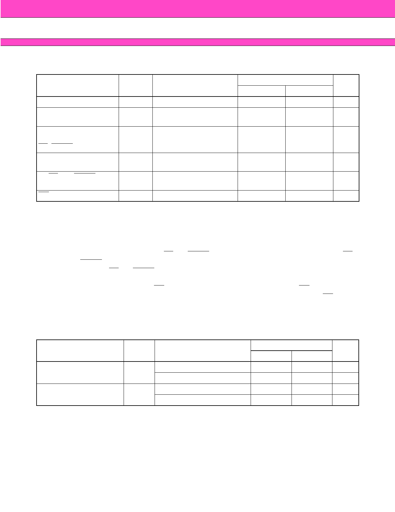
s ABSOLUTE MAXIMUM RATINGS(See WARNING)
Parameter
Symbol
Storage Temperature
Ambient Temperature with
Power Applied
Voltage with Respect to
Ground All pins except A9,
OE, RESET (Note 1)
Power Supply Voltage
(Note 1)
A9, OE, and RESET
(Note 2)
WP/ACC (Note 3)
Tstg
TA
VIN, VOUT
VCC
VIN
VIN
Conditions
Rating
Unit
Min.
Max.
–55
+125
°C
–40
+85
°C
–0.5
VCC+0.5
V
–0.5
+4.0
V
–0.5
+13.0
V
–0.5
+10.5
V
WARNING: Semiconductor devices can be permanently damaged by application of stress (voltage, current,
temperature, etc.) in excess of absolute maximum ratings. Do not exceed these ratings.
Notes: 1. Minimum DC voltage on input or I/O pins are –0.5 V. During voltage transitions, inputs may negative
overshoot VSS to –2.0 V for periods of up to 20 ns. Maximum DC voltage on output and I/O pins are VCC
+0.5 V. During voltage transitions, outputs may positive overshoot to VCC +2.0 V for periods of up to 20 ns.
2. Minimum DC input voltage on A9, OE and RESET pins are –0.5 V. During voltage transitions, A9, OE
and RESET pins may negative overshoot VSS to –2.0 V for periods of up to 20 ns. Maximum DC input
voltage on A9, OE and RESET pins are +13.0 V which may positive overshoot to 14.0 V for periods of
up to 20 ns. when VCC is applied.
3. Minimum DC input voltage on WP/ACC pin is –0.5 V. During voltage transitions, WP/ACC pin may
negative overshoot VSS to –2.0 V for periods of up to 20 ns. Maximum DC input voltage on WP/ACC pin
iis +10.5V which may positive overshoot to +10.5V for periods of up to 20ns when Vcc is applied.
s RECOMMENDED OPERATING CONDITIONS
Parameter
Ambient Temperature
Symbol
Conditions
MBM29DL32XTD/BD-80
TA
MBM29DL32XTD/BD-90/12
Value
Unit
Min.
Max.
–20
+70
°C
–40
+85
°C
Power Supply Voltage
MBM29DL32XTD/BD-80
VCC
MBM29DL32XTD/BD-90/12
+3.0
+3.6
V
+2.7
+3.6
V
Operating ranges define those limits between which the functionality of the devices are guaranteed.
WARNING: The recommended operating conditions are required in order to ensure the normal operation of the
semiconductor device. All of the device’s electrical characteristics are warranted when the device is
operated within these ranges.
Always use semiconductor devices within their recommended operating condition ranges. Operation
outside these ranges may adversely affect reliability and could result in device failure.
No warranty is made with respect to uses, operating conditions, or combinations not represented on
the data sheet. Users considering application outside the listed conditions are advised to contact their
FUJITSU representatives beforehand.
10
Share Link: 