AMS2026 Просмотр технического описания (PDF) - Advanced Monolithic Systems Inc
Номер в каталоге
Компоненты Описание
Список матч
AMS2026 Datasheet PDF : 5 Pages
| |||
AMS2026
PIN FUNCTIONS
Pin Name
Enable
/EN (A/B)
Ground GND
Input
IN
Error Flag ERROR (A/B)
Output
OUT(A/B)
Pin No.
1/4
6
7
2/3
6-8
I/O
I
I
I
O
O
Description
Enable Input, Logic turns power switch on.
Ground.
Power switch input, also supplies IC’s internal circuitry.
Overcurrent, Over temperature, Logic output.
Power switch output.
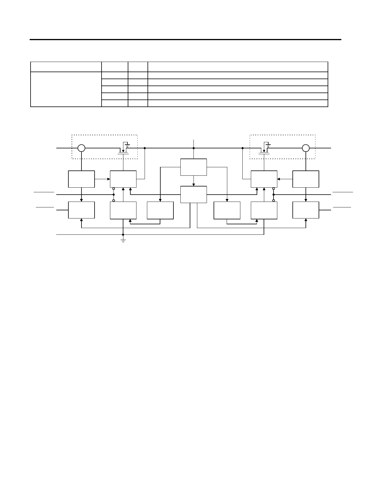
BLOCK DIAGRAM
*
OUT A
CS
POWER SWITCH
POWER SWITCH
IN
*
CS
OUT B
ENABLE A
ERROR A
CURRENT
LIMIT
ERROR
FLAG
GATE
DRIVER
CHARGE
PUMP
1.2V
REFERENCE
UVLO
THERMAL
SENSE
UVLO
GATE
DRIVER
CHARGE
PUMP
CURRENT
LIMIT
ERROR
FLAG
ENABLE B
ERROR B
GND
*Current Sense
FUNCTIONAL DESCRIPTION
Power Switch
The power switch is an N-channel MOSFET with a maximum on-
state resistance of 140mΩ (VI(IN) = 5.0V, configured as a high-
side switch.
Charge Pump
An internal 100kHz charge pump supplies the power to the driver
circuit and provides the required voltage to pull the gate of the
MOSFET above the source. The charge pump requires very little
supply current and operates from input voltages as low as 3.0V.
Gate Driver
The driver controls the gate voltage of the power switch. The
driver incorporates circuitry that controls the rise and fall times of
the output voltage, as a result it limits large current surges and
reduces the associated electromagnetic interference (EMI)
produced. The rise and fall times of the output voltage are
typically in the 2ms to 4ms range instead of the microsecond or
nanosecond range for a standard FET.
Enable
A logic high on the /EN input turns off the power switch and the
bias for the charge pump, driver, and other circuitry to reduce the
supply current to less than 10µA. A logic zero input restore bias
to the drive and control circuits and turns the power on. The
enable input is compatible with both TTL and CMOS logic
levels.
Error Flag
The error flag output, is an open drain logic output that is active
low when output current exceeds current limit. Until the fault
condition is removed the output will remain active low.
Current Limit
A sense FET monitors the current supplied to the load. In case of
an overload or short circuit, the current limit circuitry sends a
signal to the driver. The driver will then reduce the gate voltage
and drive the power FET into its linear region, which switches
the output into a constant current mode and holds the current
constant while varying the voltage on the load.
Thermal Shutdown
The internal thermal shutdown circuit will shut the power switch
off when the junction temperature rises to approx. 180°C.
Hysteresis is build into the thermal sense circuitry, and after the
junction temperature has dropped about 20°C, the switch turns
back on. Until the fault is removed the switch will continue to
cycle off and on.
Undervoltage Lock-out
An internal voltage sense monitors the input voltage. When the
input voltage is below 3.2V nominal, the switch is turned off by a
control signal. The typical fall time range due to the sense of a
low voltage is 250µs to 750µs.
Advanced Monolithic Systems, Inc. 6680B Sierra Lane, Dublin, CA 94568 Phone (925) 556-9090 Fax (925) 556-9140
Share Link: 