OZ6812 Просмотр технического описания (PDF) - O2Micro International
Номер в каталоге
Компоненты Описание
Список матч
OZ6812 Datasheet PDF : 13 Pages
| |||
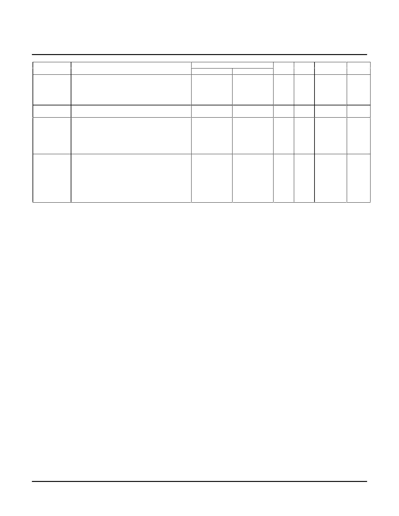
Pin Name
VPPD0/
SLATCH
VPPD1
VCCD0#/
SDATA
VCCD1#/
SCLK
Description
VPPD0: This power input is used with parallel
power control chip
SLATCH: This output controls a serial interface
power control chip.
VPPD1: This power input is used a parallel
power interface chip.
VCCD0#: Rail power inputs for use with a
parallel power control chip.
Serial Data: This pin serves as output DATA pin
when used with a serial interface of serial power
control chip.
VCCD1#: Rail power inputs for use with a
parallel power control chip.
Serial Clock: The input is used as a reference
clock (10-100kHz, usually 32kHz) to control a
serial power control chips. By setting PCI
O2Micro Control 2 register (Offset:D4h) bit 13 to
1, SCLK is an output. Default is input mode.
Pin Number
LQFP
BGA
71
M11
72
L11
73
N13
74
M12
OZ6812
Input Type
TTL I/O
Power
Rail
Aux_Vcc
Drive
12mA
-
TO Aux_Vcc 12mA
TTL I/O Aux_Vcc 12mA
TTL I/O Aux_Vcc 12mA
OZ6812-SF-1.5
Page 6
Share Link: 