ICS671M-01 Просмотр технического описания (PDF) - Integrated Circuit Systems
Номер в каталоге
Компоненты Описание
Список матч
ICS671M-01 Datasheet PDF : 4 Pages
| |||
ICS671-01
Zero Delay, Low Skew Buffer and Multipler
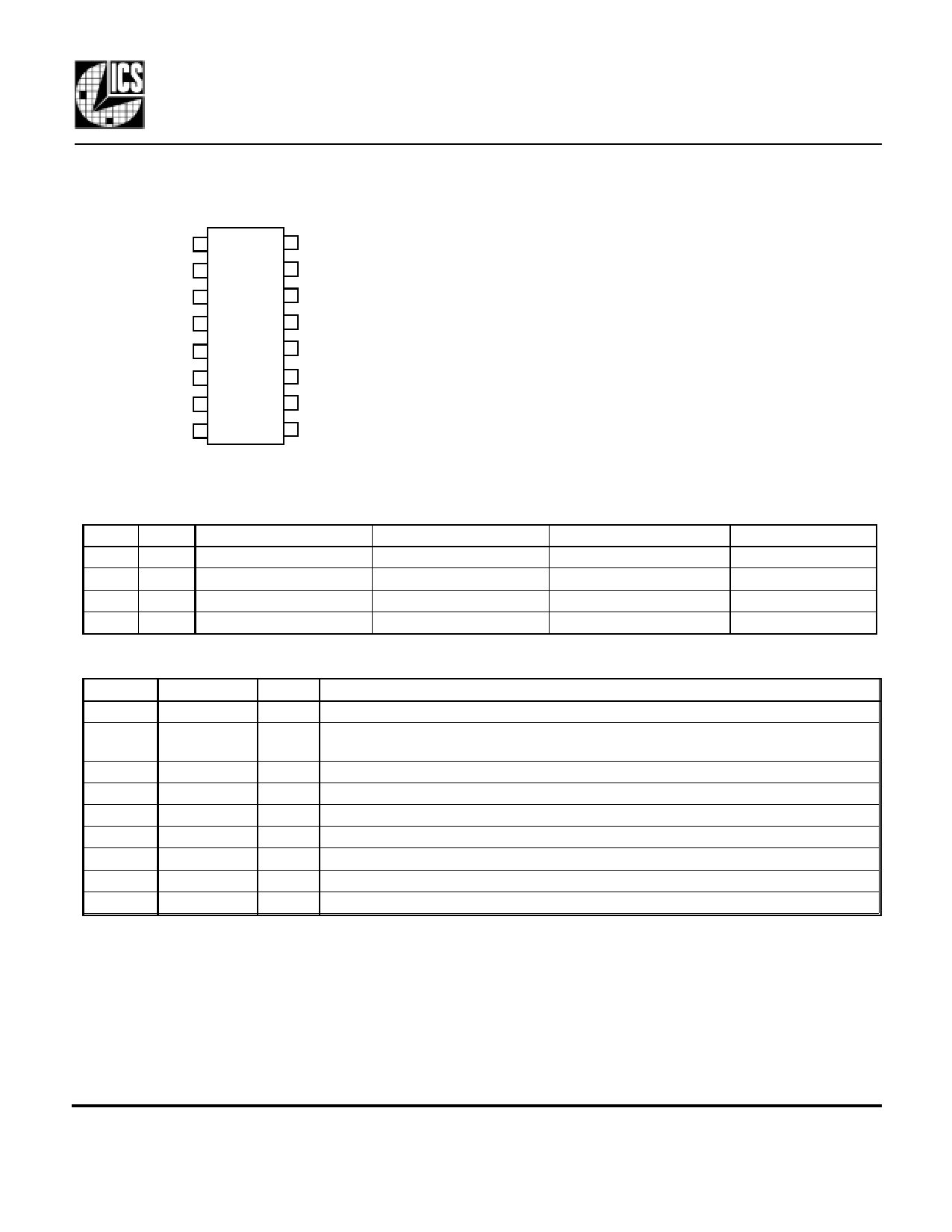
Pin Assignment
ICS671-01
CLKIN 1
CLK1 2
CLK2 3
16 FBIN
15 CLK8
14 CLK7
VDD 4
GND 5
CLK3 6
13 VDD
12 GND
11 CLK6
CLK4 7
S0 8
10 CLK5
9 S1
16 pin narrow (150 mil) SOIC
Output Clock Mode Select Table
S1
S0
CLK1:6
CLK7
CLK8
0
0 Tri-state (high impedance) Tri-state (high impedance) Tri-state (high impedance)
0
1
x2
x5
x1
1
0
x2
x2
x2
1
1
x4
x4
x4
Input range
-
5 to 30 MHz
15 to 80 MHz
7.5 to 40 MHz
Pin Descriptions
Number
1
2, 3, 6, 7,
10, 11
4, 13
5, 12
8
9
14
15
16
Name
CLKIN
CLK1:6
VDD
GND
S0
S1
CLK7
CLK8
FBIN
Type Description
I Clock Input.
O Clock Outputs 1:6. See above table.
P Power supply. Connect both pins to same voltage (either 3.3 V or 5 V).
P Connect to ground.
I Select input 0. See table above.
I Select input 1. See table above.
I Clock Output 7. See table above.
I Clock Output 8. See table above. Normally use this clock as feedback.
I Feedback Input. Connect to CLK8 under normal operations.
Key: I = Input; O = output; P = power supply connection.
External Components
The ICS671-01 requires a minimum number of external components for proper operation. Decoupling
capacitors of 0.01µF should be connected between VDD and GND on pins 4 and 5, and VDD and GND
on pins 13 and 12, as close to the device as possible. A series termination resistor of 33 Ω may be used close
to each clock output pin to reduce reflections.
MDS 671-01 B
2
Revision 051700
Printed 11/15/00
Integrated Circuit Systems, Inc.• 525 Race Street • San Jose •CA•95126• (408) 295-9800 tel • www.icst.com
Share Link: 