PBL38813 Просмотр технического описания (PDF) - Ericsson
Номер в каталоге
Компоненты Описание
Список матч
PBL38813 Datasheet PDF : 16 Pages
| |||
PBL 388 13
RE 22
RDC 21
CTR 24
Txout 4
V+ 15
3
5
–
+
+
F3
-C
LSP +L VOL
17 18
20
19
PBL 388 13
Control
F6
23 LSPin
16 GND
11 Rxout
12
10
F2
-Txin 1 -
+Txin
2
F1
+
7
N Det R5
+
C4
6
8
TxDet CMP
Ref.
9
RxDet
+
C3
+
C1 C2
F5
14 -Rxin
F4
+ 13 +R xin
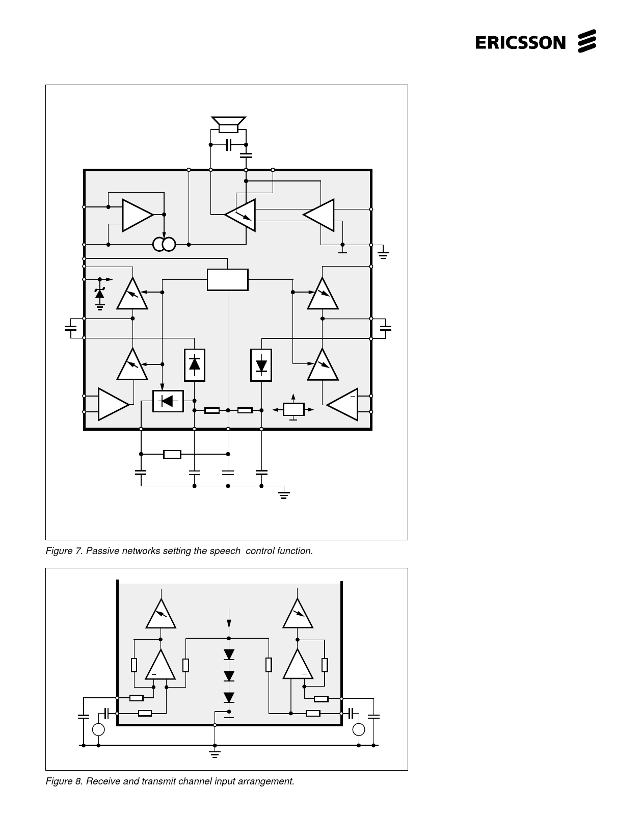
Figure 7. Passive networks setting the speech control function.
PBL388 13
F2
100k 100k
F1 +
3k
Tx
1
3k
2
~ VTxin
I
Ref.
16
F5
120k 120k
F4
+
20k
20k 14
Rx
13
~ VRxin
Figure 8. Receive and transmit channel input arrangement.
6
Functional Description
Speech control section
Transmitter and Receiver
Channels
The transmitter and receiver channels
consist of three amplifying stages each, F1,
F2, F3 and F4, F5, F6. The inputs of the
amplifiers must be ac. coupled because
they are dc. vise at the internal reference
voltage (≈ 2V) level. F1 and F4 are fixed
gain amplifiers of 29.5 dB and 15.5 dB
respectively, while the rest of them are of
controlled gain type amplifiers.The gain of
F2, F3 as well as F5 and F6 is controlled by
the comparator. Ac. loading the channel
outputs F3 and F6 will lessen the dc.
current consumption, maximum load 10
kΩ. The output capacity can be increased
somewhat in case needed, by coupling a
10 kΩ resistor from the respective output
pin directly to ground (before the optional
capacitor).The comparator receives its in-
formation from the summing point of the
transmitter, receiver and background noise
detectors at CMP input. The control input
CTR, controls the gain dynamics (25 or 50
dB). Amplifiers F2 and F3 have the maxi-
mum gain when the transmitter channel is
fully open, consequently the amplifiers F5
and F6 will have minimum gain and vice
versa. See figure 7 and figure 13.
The positive input on each channel
has a high input impedance. It renders a
good gain precision and noise performance
when used with low impedance signal
source . The negative input of the receiver
channel should be returned to ground with
a capacitor. The differential input of the
transmitter channel can be used to sup-
press unwanted signals in the microphone
supply, see figure 9. Also see application.
Signal Detectors and the
Comparator
The signal detectors sense and rectify
the receiver and microphone signals to
opposite polarities referenced to the internal
reference voltage of approx. 2V. The voltage
at RxDet will go positive and at TxDet
negative in the presence of a signal at the
respective channel input. In the idle (no
signal) state, the voltages at RxDet ,TxDet
and CMP are equal to the internal reference
voltage. Signal at Txin will result in a
decreasing level at TxDetout and hence
also at CMP input.
Share Link: 