SL34118 Просмотр технического описания (PDF) - System Logic Semiconductor
Номер в каталоге
Компоненты Описание
Список матч
SL34118 Datasheet PDF : 12 Pages
| |||
SL34118
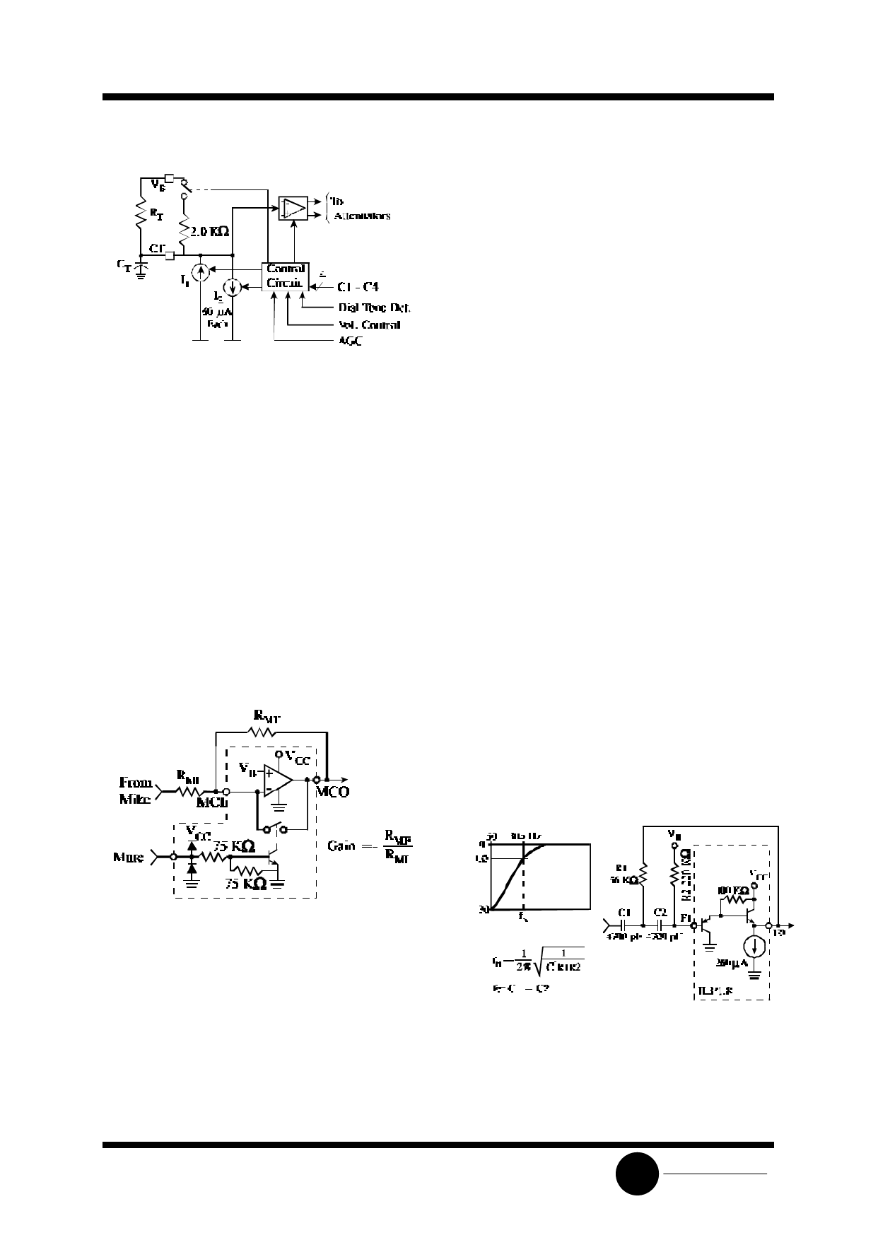
Figure 4. CT Attenuator Control Block Circuit
MICROPHONE AMPLIFIER
The microphone amplifier (Pin 10, 11) has the
noninverting input internally connected to VB, while
the inverting input and the output are pinned out.
Unlike most op-amps, the amplifier has an all-NPN
output stage, which maximizes phase margin and
gain-bandwidth. This feature ensures stability at
gains less than unity, as well as with a wide range of
reactive loads. The open loop gain is typically 80 dB
(f<100 Hz), and the gain-bandwidth is typically
1.0 MHz. The maximum p-p output swing is typically
1.0 volt less than VCC with an output impedance of
<10 Ω until curent limiting is reached (typically
1.5 mA). Input bias current at MCI is typically 40 nA
out of the pin.
Figure 5. Microphone Amplifier and MUTE
HYBRID AMPLIFIERS
The two hybrid amplifiers (at HTO+, HTO-, and
HTI), in conjunction with an external transformer,
provide the two-to-four wire converter for interfacing
to the telephone line. The gain of the first amplifier
(HTI to HTO-) is set by external resistors (gain = -
RHF/RHI in Figure 8), and its output drives the second
amplifier, the gain of which is internally set at -1.0.
Unlike most op-amps, the amplifiers have an all-NPN
output stage, which maximizes phase margin and
gain-bandwidth. This feature ensures stability at
gains less than unity, as well as with a wide range of
reactive loads. The open loop gain of the first
amplifier is typically 80 dB, and the gain bandwidth of
each amplifier is ≈1.0 MHz. The maximum p-p output
swing of each amplifier is typically 1.2 volts less than
VCC with an output impedance of <10 Ω until current
limiting is reached (typically 8.0 mA). The output
current capability is guaranteed to be a minimum of
5.0 mA. The bias current at HTI is typically 30 nA out
of the pin.
The connections to the coupling transformer are
shown in the Expanded Logic Diagram (Figure 8). The
block labeled Zbal is the balancing network necessary
to match the line impedance.
FILTER
The operation of the filter circuit is determined by
the external components. The circuit within the
IL34118, from pins FI to FO is a buffer with a high
input impedance (>1.0 MΩ), and a low output
impedance (<50 Ω). The configuration of the external
components determines whether the circuit is a high-
pass filter (as shown in Figure 8), a low-pass filter, or
a band-pass filter.
Figure 6. High Pass Filter
The muting function (Pin 12), when activated, will
reduce the gain of the amplifier to = -39 dB (will RMI
= 5.1 KΩ) by shorting the output to the inverting
input (see Figure 5). The mute input has a threshold
of 1.5 volt, and the voltage at this pin must be kept
withing the range of ground and VCC. If the mute
function is not used, the pin should be grounded.
As a high pass filter, with the components shown in
Figure 6 the filter will keep out 60 Hz (and 120 Hz) hum
which can be picked up by the external telephone
lines.
SLS
System Logic
Semiconductor
Share Link: 