CMX624 Просмотр технического описания (PDF) - CML Microsystems Plc
Номер в каталоге
Компоненты Описание
Список матч
CMX624 Datasheet PDF : 26 Pages
| |||
V23 / Bell 202 Modem
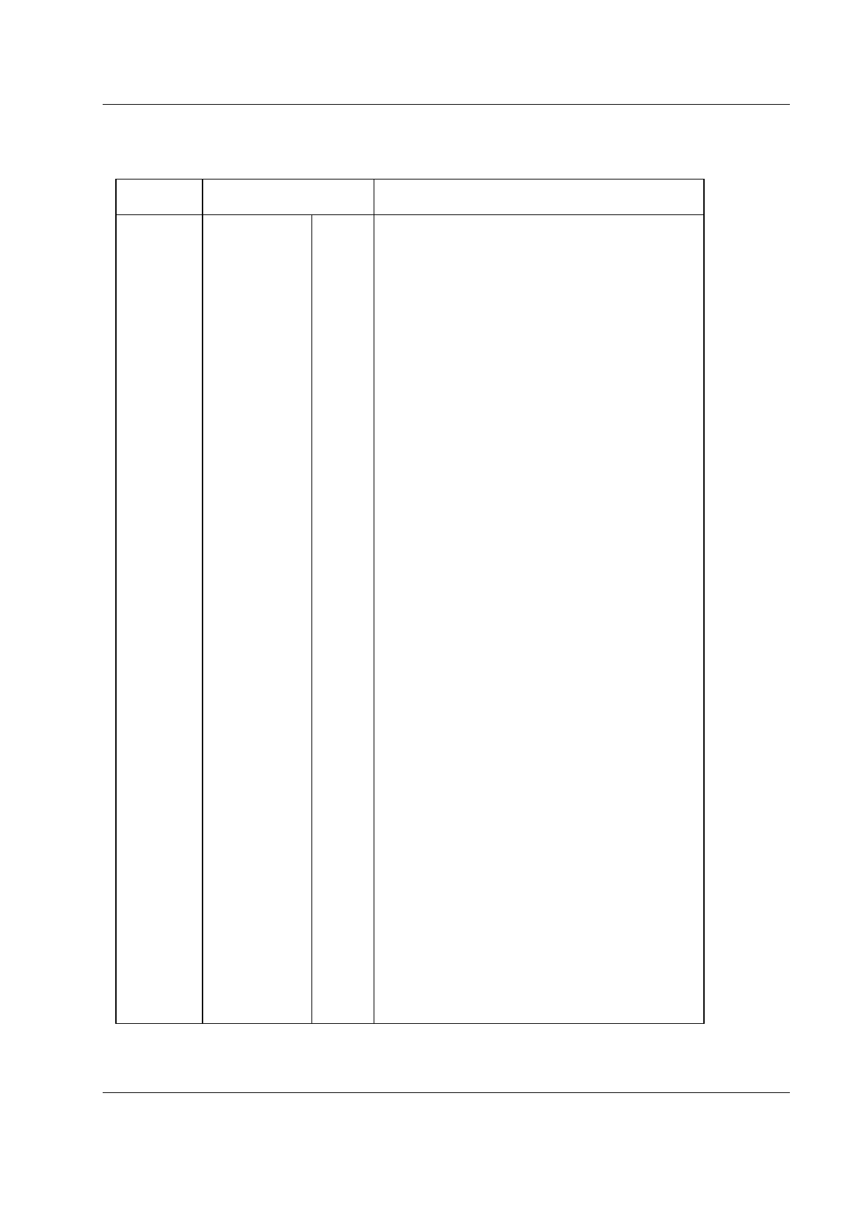
1.3 Signal List
CMX624
D2/D5/P4
Signal
Description
Pin No.
1
2
3
4
5
6
7
8
9
10
11
12
13
14
15
Name
Type
XTALN
O/P The output of the on-chip Xtal oscillator inverter.
XTAL/CLOCK I/P The input to the oscillator inverter from the Xtal
circuit or external clock source.
SERIAL
CLOCK
I/P The ‘C-BUS’ serial clock input from the µC. See
Section 1.5.11
COMMAND
DATA
I/P The ‘C-BUS’ serial data input from the µC.
REPLY DATA T/S A 3-state ‘C-BUS’ serial data output to the µC.
This output is high impedance when not sending
data to the µC.
CSN
IRQN
I/P The ‘C-BUS’ transfer control input provided by
the µC.
O/P A ‘wire-ORable’ output for connection to a µC
Interrupt Request input. This output is pulled
down to Vss when active and is high impedance
when inactive. An external pullup resistor is
required.
TOP
TXO
TXN
TXON
VSS
VBIAS
O/P
O/P
I/P
O/P
Power
O/P
The Tx analogue signal output.
The output of the line driving amplifier.
The inverting input to the line driver amplifier.
The inverted output of the line driving amplifier.
The negative supply rail (ground).
Internally generated bias voltage of VDD/2,
except when the device is in ‘Zero Power’ mode
when VBIAS will discharge to VSS. Should be
decoupled to VSS by a capacitor mounted close
to the device pins.
RLYDRV
O/P Relay drive open drain output. This output is
pulled down to VSS when active and is high
impedance when inactive.
RXP
I/P The non-inverting input to the Rx input amplifier.
CMX624
2003 CML Microsystems Plc
4
D/624/7
Share Link: 