L6213 Просмотр технического описания (PDF) - STMicroelectronics
Номер в каталоге
Компоненты Описание
Список матч
L6213 Datasheet PDF : 9 Pages
| |||
L6213
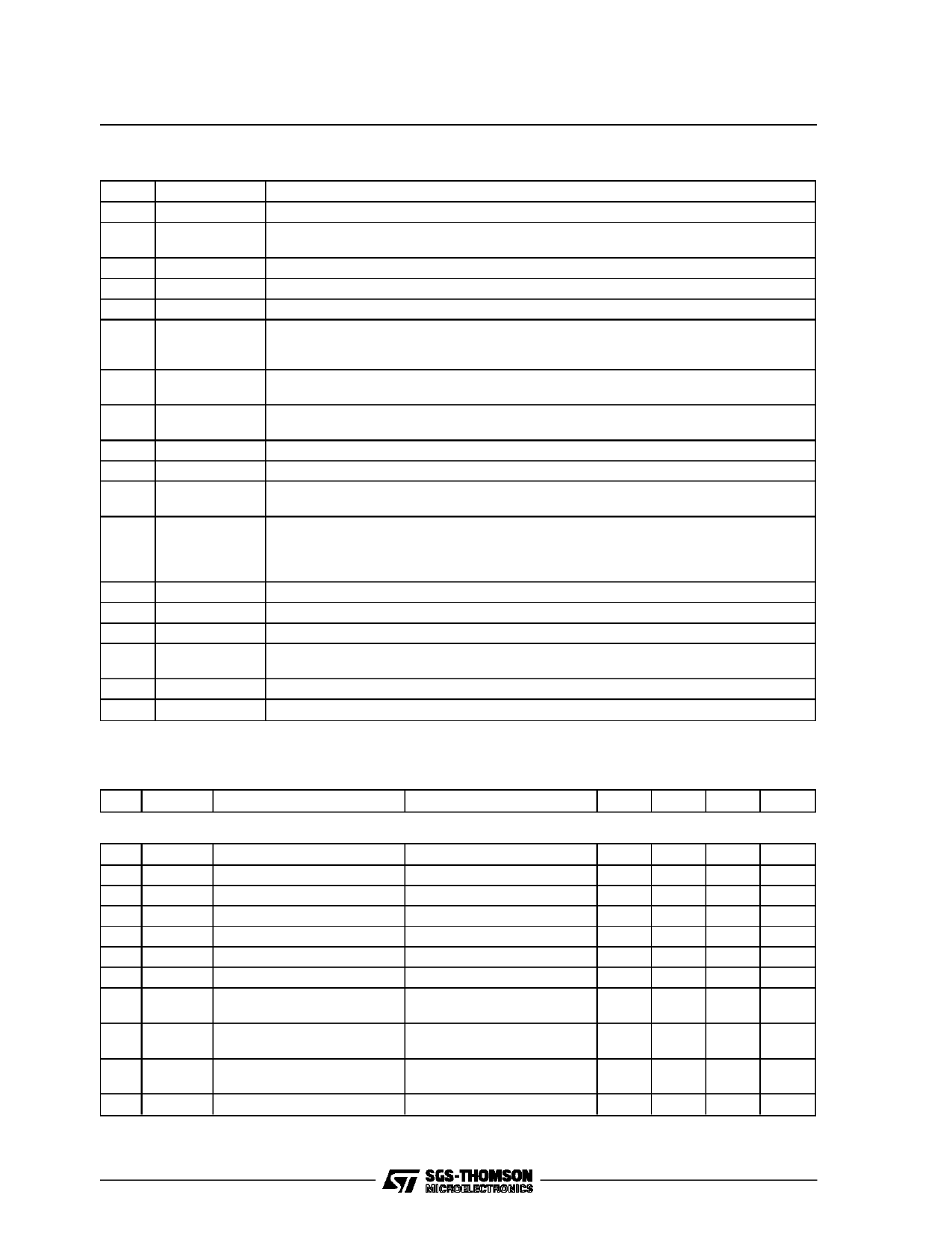
PIN DESCRIPTION
Nr.
Name
1
Out-Up
2
BSE
3
ENABLE
4
+VS1
5, 6
GND
7
PF
8
PFP
9
CD
10
VS2
11
VD
12
BSA
13
RESET
14
15, 16
17
18
19
20
Vout
GND
Rsense
PIM
ISTP
Out-Down
Description
Solenoid section upper DMOS output.
Solenoid section upper DMOS bootstrap. A capacitor connected between pin 2 and pin 1
ensures the efficient driving of the solenoid section upper DMOS.
Solenoid control input - TTL compatible.
Unregulated voltage input - Solenoid section.
Ground.
Power fail output, the saturation of PF is guaranteed if VPS exceed 3V. PF is at logic 1 a
time T1 after RESET reached the high level. PF came back to logic 0 when VPS goes
down under 18V. (see fig. 1)
Power fail programming. A resistor divider connected to VPS changes the Power fail
threshold levels.
Capacitor delay. A capacitor connected to this pin determines the Reset signal delay time
td.
Unregulated voltage input - SMPS sections.
Regulator output and diode voltage control.
SMPS section DMOS bootstrap. A capacitor connected between pin 12 and pin 11
ensures efficient driving of SMPS DMOS.
Reset output. The saturation of Reset is guaranteed if VPS exceeds 3V. The Reset output
reaches the logic level 1 a time delay (set by capacitor CD) after VPS has reached a
rising threshold voltage. Reset reaches 0 level when VPS goes down below folling
threshold.
Feed back input of the regulation loop.
Ground.
Connection for solenoid sensing resistor.
Programming of solenoid current rising edge. An RC network connected to this pin
determines the slope of the solenoid current rising edge.
Programming of solenoid current histeresys.
Solenoid section lower DMOS output.
ELECTRICAL CHARACTERISTICS (Refer to the application circuit, TJ =25°C, Iout Power Supply =
50mA, VPS from 12V to 46V; unless otherwise specified.
Pin Symbol
Parameter
STEP-DOWN SECTION
Test Condition
Min. Typ. Max. Unit
10, 4
Vi
Supply Voltage
14
46
V
14
Vo
Output Voltage
IO = 0.05 to 1A
4.85
5.2
V
RDS on On State Drain Resistance
TJ = 25°C; VPS = 15 to 46V
0.56 0.7
Ω
10
th on
Turn-on Threshold
VPS Rising Fig. 1
10
12
V
10
th off
Turn-off Threshold
VPS Falling Fig. 1
10
12
V
10
IB
Input Bias Current
15
mA
11
Ilim
Static Current Limiting
2.2
3.4
A
2, 10
Ii
Total Input Current
ENABLE = 1, VPS = 46V,
Iload = 0
13
mA
2, 10
Ii
Total Input Current
ENABLE = 1, VPS = 15V,
Iload = 0
18
mA
11
td p
Protection Current Maximum
Delay Time
1
µs
to ff
Minimum Power off State
VPS = 46V IO = 50mA
4.2
7.8
µs
4/9
Share Link: 