LTC1694 Просмотр технического описания (PDF) - Linear Technology
Номер в каталоге
Компоненты Описание
Список матч
LTC1694 Datasheet PDF : 8 Pages
| |||
LTC1694
ABSOLUTE AXI U RATI GS
(Note 1)
Supply Voltage (VCC) ................................................. 7V
SMBus1, SMBus2 Inputs ............ – 0.3V to (VCC + 0.3V)
Operating Ambient Temperature Range
LTC1694C ............................................... 0°C to 70°C
LTC1694I ............................................ – 40°C to 85°C
Junction Temperature ........................................... 125°C
Storage Temperature Range ................. – 65°C to 150°C
Lead Temperature (Soldering, 10 sec).................. 300°C
UW U
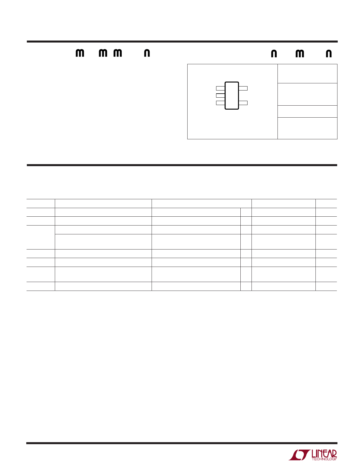
PACKAGE/ORDER I FOR ATIO
TOP VIEW
ORDER PART
NUMBER
VCC 1
GND 2
NC 3
5 SMBus1
4 SMBus2
S5 PACKAGE
5-LEAD PLASTIC TSOT-23
TJMAX = 125°C, θJA = 256°C/ W
LTC1694CS5
LTC1694IS5
S5 PART MARKING
LTEE
LTA8
Consult LTC Marketing for parts specified with wider operating temperature ranges.
ELECTRICAL CHARACTERISTICS
The q denotes specifications that apply over the full operating temperature range, otherwise specifications are at TA = 25°C.
VCC = 2.7V to 6V unless otherwise noted.
SYMBOL
PARAMETER
CONDITIONS
MIN TYP MAX
UNITS
VCC
ICC
IPULL-UP
VTHRES
SRTHRES
tr
Supply Voltage Range
Supply Current
Pull-Up Current
Boosted Pull-Up Current
Input Threshold Voltage
Slew Rate Detector Threshold
SMBus Rise Time
Standard Mode I2C Bus Rise Time
2.7
6
V
SMBus1 = SMBus2 = Open
q 20
60
100
µA
SMBus1 = SMBus2 = 0V
q 125
275
350
µA
Positive Transition on SMBus ( Figure 1) q 1.0
2.2
mA
Slew Rate = 0.5V/µs, SMBus > VTHRES
Slew Rate = 0.5V/µs (Figure 1)
q 0.4
0.65
0.9
V
SMBus > VTHRES
q
Bus Capacitance = 200pF (Note 2)
q
Bus Capacitance = 400pF (Note 3)
q
0.2
0.5
V/µs
0.32 1.0
µs
0.30 1.0
µs
fMAX
SMBus Maximum Operating Frequency
(Note 4)
q
100
kHz
Note 1: Absolute Maximum Ratings are those values beyond which the life
of a device may be impaired.
Note 2: The rise time of an SMBus line is calculated from (VIL(MAX) –
0.15V) to (VIH(MIN) + 0.15V) or 0.65V to 2.25V. This parameter is
guaranteed by design and not tested. With a minimum pull-up current of
125µA, a minimum boosted pull-up current of 1mA and a maximum input
threshold voltage of 0.9V:
Rise Time = [(0.9V – 0.65V)/125µA + (2.25V – 0.9V)/1mA] • 200pF
= 0.67µs
Note 3: The rise time of an I2C bus line is calculated from VIL(MAX) to
VIH(MIN) or 1.5V to 3V (with VCC = 5V). This parameter is guaranteed by
design and not tested. With a minimum boosted pull-up current of 1mA:
Rise Time = (3V – 1.5V) • 400pF/1mA = 0.6µs
Note 4: This parameter is guaranteed by design and not tested.
1694fa
2
Share Link: 