CDP1020 Просмотр технического описания (PDF) - Intersil
Номер в каталоге
Компоненты Описание
Список матч
CDP1020 Datasheet PDF : 23 Pages
| |||
CDP1020
SECURE Inputs
The SECURE0 and SECURE1 inputs are used by the
CDP1020 to monitor the state of an external device security
lock. The purpose of this lock is to prevent unauthorized
removal or theft of a device in a device bay system. Like the
REMREQ inputs, this is an optional feature of the device bay
system. Typical connection of the SECURE inputs is shown
in Figure 18.
Like the presence and REMREQ inputs, the SECURE inputs
implement internal active pull-up devices. When the security
lock is disengaged (i.e., the device may be removed from the
bay), the lock switch should be in an open state, thus
rendering the SECURE input at a logic high level. When the
lock is engaged, the lock switch should then close and pull
the SECURE input to ground. If the security lock function of
the device bay system is not implemented, these pins should
be tied to VDD of the CDP1020.
Address Select Pins AD1 and AD0
The address select pins are used by the CDP1020 as the
lower two bits of its 7-bit I2C/SMBus slave address. By
making these two pins configurable externally, up to four
CDP1020 devices can share the common bus. The upper
five bits of the I2C/SMBus address are internally hard-wired
to %10010xx. Note that the R/W bit can be considered the
8th bit (LSB) in the address.
The AD0 and AD1 pins should be connected to the VDD or
the VSS power supplies of the CDP1020, as appropriate.
They should not be left floating; doing so will cause the
CDP1020 to randomly configure its slave address on power-
up. These pins are sampled immediately after reset.
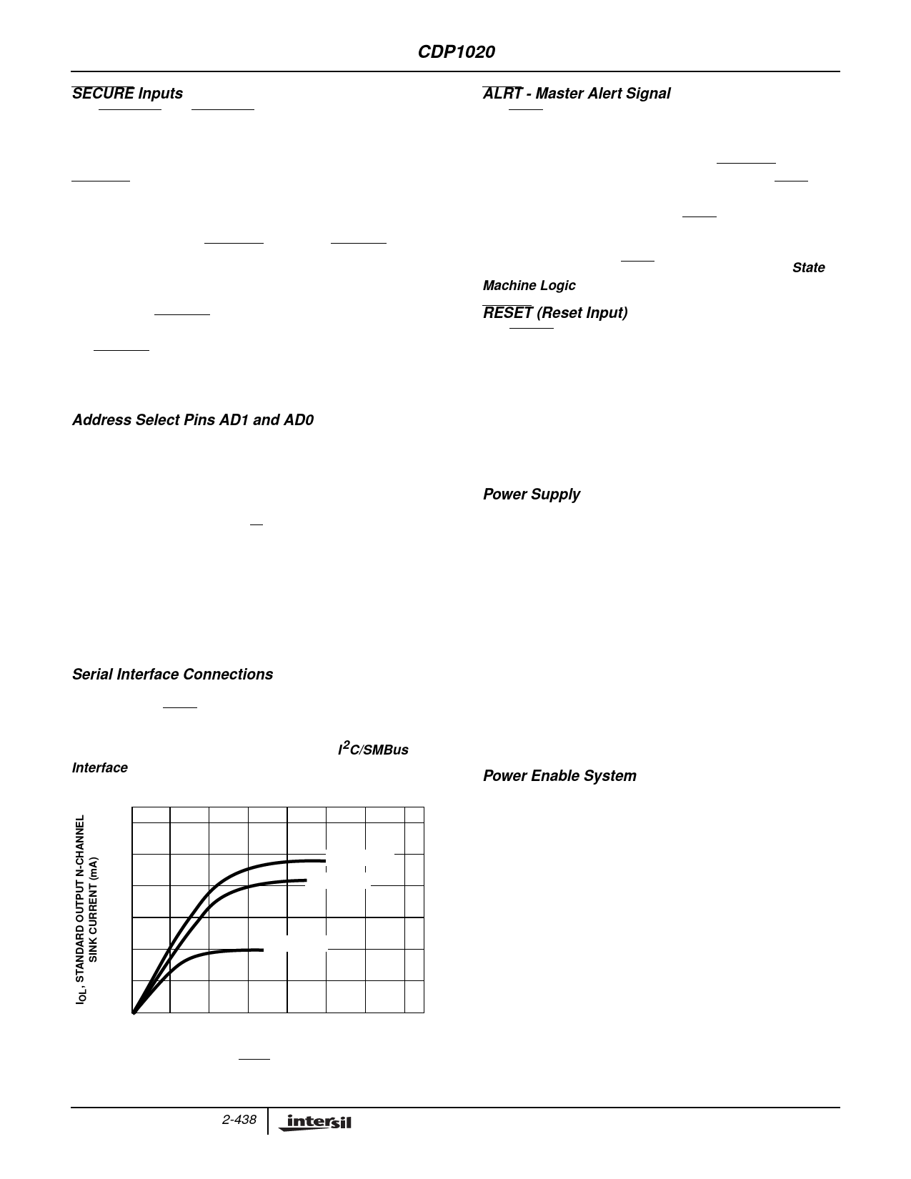
Serial Interface Connections
The serial interface connections of the CDP1020 include the
SDA, SCK and ALRT pins. All three of these pins are open-
drain when in the output mode and are +5V tolerant. The
functionality of these pins is described in the I2C/SMBus
Interface text. Typical drive characterization is shown in
Figure 13.
30.0
25.0
VDD = 5.0V
20.0
VDD = 4.5V
15.0
10.0
VDD = 3.3V
5.0
0
1.0 2.0 3.0 4.0 5.0 6.0
VO, OUTPUT VOLTAGE (V)
FIGURE 13. SDA, SCK AND ALRT OUTPUT N-CHANNEL SINK
CURRENT AT 25oC
ALRT - Master Alert Signal
The ALRT pin of the CDP1020 is an open drain output used
to signal the I2C/SMBus master that a device state change
has occurred and that this state should be processed by the
operating system. Unlike the presence, REMREQ and
security inputs, there is no internal pull-up on the ALRT pin.
As such, there needs to be one present in the external
system. Typical connection of the ALRT pin is shown in
Figure 18.
The functionality of the ALRT pin is described in the State
Machine Logic text.
RESET (Reset Input)
The RESET pin can be connected in the following ways:
• If not used, must be tied to VDD.
• Connected to a system reset (such as from the PiiX4
South Bridge). Be sure it is an active low polarity.
• Connected to an external RC (Resistor to VDD, Capacitor
to Ground), to act as an additional power-on reset. The
time constant should be chosen to be longer than the turn-
on ramp of the VDD power supply used.
Power Supply
The power supply input for the CDP1020 are the VDD
(positive) and VSS (negative) pins. The VSS pin should be
connected to the system ground. The VDD pin should be
connected to a positive power supply from +3.3V to +5.0V.
There are few differences in performance between voltages;
in general, the higher voltage will allow more output drive
current (LED pins, but the current should be limited by an
external resistor anyway), and a higher gate voltage for the
SFTLOCK pins (driving Logic-Level FETs). However, the
higher voltage may also consume a higher supply current
(the amount of available supply current may help decide
which one to use). Keep in mind that the Oscillator RC needs
to be chosen to match the VDD (in order to get the optimal
4MHz frequency).
Power Enable System
The Power Enable System enables the CDP1020 to directly
drive the gate of the VID control MOSFETs. Logically, the
PWRENx output matches the state of the PWR_CTLx bit in
the corresponding BCER register. However, instead of being
a logic level CMOS output, the PWREN outputs are “level-
shifted” such that their output current is supplied directly
from the VGATE power input pin.
When the PWR_CTL bit is a logic 0, the PWREN output will
sink current to VSS through its N-Channel output driver.
However, when the PWR_CTL bit is a logic 1, the PWREN
output will source current, limited to a maximum of 25µA,
from the VGATE power input. The VGATE input is typically
tied to the +12V power supply of the system. Figure 14
shows a block diagram of this system.
2-438
Share Link: 