SP6642EU Просмотр технического описания (PDF) - Signal Processing Technologies
Номер в каталоге
Компоненты Описание
Список матч
SP6642EU Datasheet PDF : 16 Pages
| |||
PERFORMANCE CHARACTERISTICS (continued)
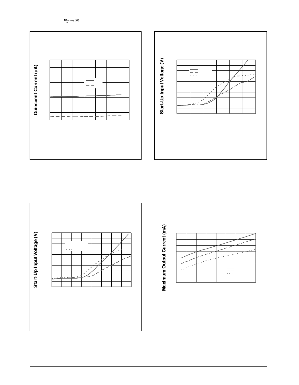
Refer
to
the
circuit
in
Figure
25
with
V
BATT
=
1.2V,
R1
+
R2
=
1MΩ,
and
T
AMB
=
+25OC
unless
otherwise
noted.
40
35
30
25
20
15
10
5
0
-40 -20
Iout
Ibatt
0 20 40 60 80 100
Temperature (oC)
1.6
1.5
1.4
1.3
1.2
1.1
1.0
0.9
0.8
0.7
0.6
0
Vout = 5V
Vout = 3.3V
Vout = 2.4V
5 10 15 20 25 30
Output Current (mA)
Figure 9. VBATT and VOUT Pin Quiescent Currents vs.
Temperature where VBATT = 1.2V, VOUT = 3.6V
Figure 10. Minimum Start-Up Input Voltage vs. Output
Current where L1=100µH, Sumida CD54-101
1.6
1.5
1.4
1.3
Vout = 5V
Vout = 3.3V
Vout = 2.4V
1.2
1.1
1.0
0.9
0.8
0.7
0.6
0 2 4 6 8 10 12 14 16
Output Current (mA)
40
35
30
25
20
15
10
5
0
0.8 0.9 1.0 1.1 1.2 1.3
Vout = 2.4V
Vout = 3.3V
Vout = 5V
1.4 1.5 1.6
Input Voltage (V)
Figure 11. Minimum Start-Up Input Voltage vs. Output
Current where L1=150µH, TDK NLC565050T-151K
Figure 12. Maximum Output Current vs. Input Voltage
where L1=100µH, Sumida CD54-101
Rev. 10-6-00
SP6642/6643 High Efficiency Step-Up DC-DC Converter
6
© Copyright 2000 Sipex Corporation
Share Link: 