HPMX-2003-T10 Просмотр технического описания (PDF) - HP => Agilent Technologies
Номер в каталоге
Компоненты Описание
Список матч
HPMX-2003-T10 Datasheet PDF : 16 Pages
| |||
HPMX-2003 NADC
Applications
The NADC System
NADC (North American Digital
Cellular) commonly refers to the
digital sections of the IS-55
cellular telephone system stan-
dard. Dual mode (FM/TDMA)
cellular phones for the North
American market must conform
to this standard. The NADC
system is characterized by 30 kHz
channel spacing and mobile to
base transmit frequencies of 824 -
849 MHz. The primary modulation
characteristics include π/4 DQPSK
filtering of the I and Q signals and
48.6 kbps transmission rate.
Critical Performance
Parameters
System specifications require that
the telephone exhibit RMS modu-
lation error under 12% in the digi-
tal mode. The modulated output
spectrum of the phone must lie
within a “spectral mask” which
defines maximum allowable radia-
tion levels into adjacent and alter-
nate channels. Specifically, total
power radiated into the either ad-
jacent channel must be at least
26␣ dB below the mean output
power. Total power radiated into
either alternate channel must be
at least 45 dB below the mean out-
put power. Refer to the IS-55
specifications for more detailed
information.
HPMX-2003 Performance
The typical RMS modulation error
level of 4% makes the HPMX-2003
an excellent choice for NADC
applications. The output falls
easily within the NADC spectral
requirements, and the high power
and simple output configuration
mean lower components count,
reduced size and higher system
efficiency.
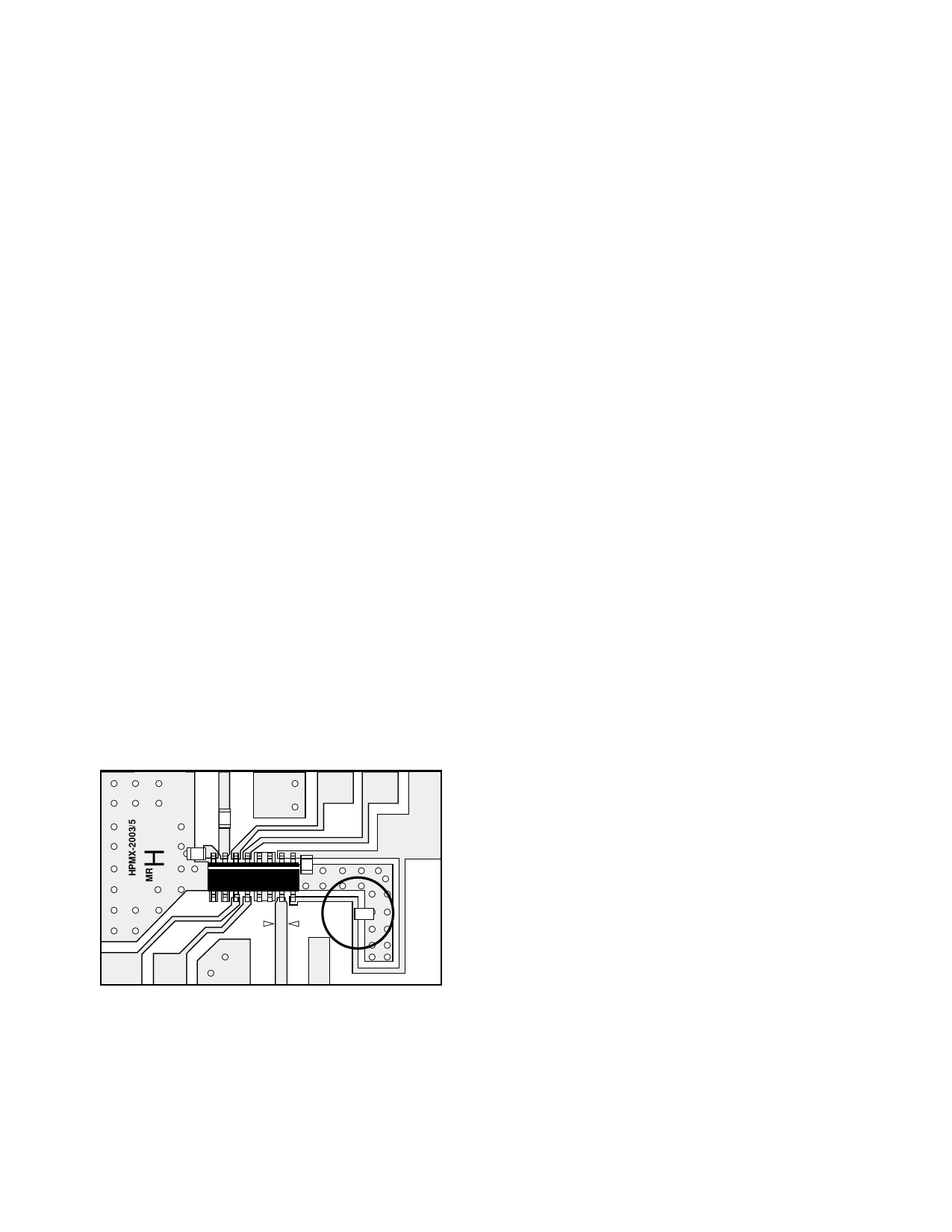
Particulars of Use
Many of the NADC application
performance graphs shown in this
data sheet were created using the
test board shown in figure 31,
below.
The only external components re-
quired by this IC are four chip
capacitors. One capacitor is used
as a DC block on the input trans-
mission line. The second capaci-
tor (at pin 8) provides an AC
ground to one side of the differen-
tial LO input. The third and fourth
capacitors (at pins 1 and 16) are
for VCC bypass.
The circuit board includes an in-
ductive trace that can optionally
be used to minimize output VSWR
by placing a bypass capacitor at
various points along the inductive
line. Minimum VSWR for NADC
applications is achieved by plac-
ing the capacitor as shown in the
circle (inductance ≈ 6 nH).
The IC has an internal blocking
capacitor so the output is a simple
50 Ω transmission line. An en-
larged scale layout of the test
board can be found on the last
page of this data sheet.
VER. 1
C
C
LO
Q
C
R
VCC
5V
C
OUT
I
R
Figure 31. HPMX-2003 NADC Test Board.
7-49
Share Link: 