HS-80C86RH(1995) Просмотр технического описания (PDF) - Intersil
Номер в каталоге
Компоненты Описание
Список матч
HS-80C86RH Datasheet PDF : 37 Pages
| |||
HS-80C86RH
RESET BOOTSTRAP
PROGRAM JUMP
FFFFFH
FFFFOH
Status bits S0, S1 and S2 are used by the bus controller, in
maximum mode, to identify the type of bus transaction
according to Table 8.
INTERRUPT POINTER
FOR TYPE 255
3FFH
3FCH
7H
INTERRUPT POINTER
FOR TYPE 1
4H
INTERRUPT POINTER
3H
FOR TYPE 0
0H
FIGURE 2. RESERVED MEMORY LOCATIONS
Minimum and Maximum Operation Modes
The requirements for supporting minimum and maximum
HS-80C86RH systems are sufficiently different that they
cannot be met efficiently using 40 uniquely defined pins.
Consequently, the HS-80C86RH is equipped with a strap pin
(MN/MX) which defines the system configuration. The defini-
tion of a certain subset of the pins changes, dependent on
the condition of the strap pin. When the MN/MX pin is
strapped to GND, the HS-80C86RH defines pins 24 through
31 and 34 in maximum mode. When the MN/MX pin is
strapped to VDD, the HS-80C86RH generates bus control
signals itself on pins 24 through 31 and 34.
Bus Operation
The HS-80C86RH has a combined address and data bus
commonly referred to as a time multiplexed bus. This tech-
nique provides the most efficient use of pins on the proces-
sor while permitting the use of a standard 40-lead package.
This “local bus” can be buffered directly and used throughout
the system with address latching provided on memory and
I/O modules. In addition, the bus can also be demultiplexed
at the processor with a single set of 82C82 latches if a stan-
dard non-multiplexed bus is desired for the system.
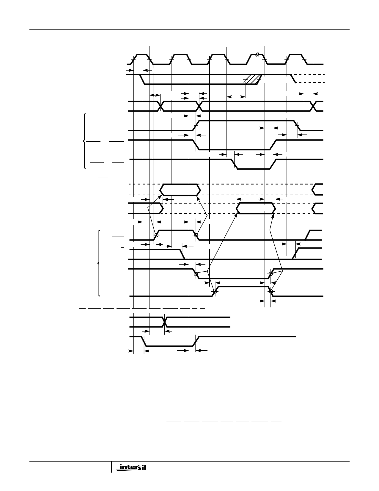
Each processor bus cycle consists of at least four CLK cy-
cles. These are referred to as T1, T2, T3 and T4 (see Figure
3). The address is emitted from the processor during T1 and
data transfer occurs on the bus during T3 and T4. T2 is used
primarily for changing the direction of the bus during read
operations. In the event that a “NOT READY” indication is
given by the addressed device, “Wait” states (TW) are
inserted between T3 and T4. Each inserted wait state is the
same duration as a CLK cycle. Idle periods occur between
HS-80C86RH driven bus cycles whenever the processor
performs internal processing.
During T1 of any bus cycle, the ALE (Address Latch Ena-
ble) signal is emitted (by either the processor or the 82C88
bus controller, depending on the MN/MX strap). At the trail-
ing edge of this pulse, a valid address and certain status
information for the cycle may be latched.
TABLE 8.
S2
S1
S0
CHARACTERISTICS
0
0
0 Interrupt Acknowledge
0
0
1 Read I/O Port
0
1
0 Write I/O Port
0
1
1 Halt
1
0
0 Instruction Fetch
1
0
1 Read Data from Memory
1
1
0 Write Data to Memory
1
1
1 Passive (no bus cycle)
Status bits S3 through S7 are time multiplexed with high
order address bits and the BHE signal, and are therefore
valid during T2 through T4. S3 and S4 indicate which seg-
ment register (see Instruction Set Description) was used for
this bus cycle in forming the address, according to Table 9.
TABLE 9.
S4
S3
CHARACTERISTICS
0 (Low) 0 Alternate Data (extra segment)
0
1 Stack
1 (High) 0 Code or None
1
1 Data
S5 is a reflection of the PSW interrupt enable bit. S6 is
always zero and S7 is a spare status bit.
I/O Addressing
In the HS-80C86RH, I/O operations can address up to a
maximum of 64K I/O byte registers or 32K I/O word regis-
ters. The I/O address appears in the same format as the
memory address on bus lines A15-A0. The address lines
A19-A16 are zero in I/O operations. The variable I/O instruc-
tions which use register DX as a pointer have full address
capability while the direct I/O instructions directly address
one or two of the 256 I/O byte locations in page 0 of the I/O
address space.
I/O ports are addressed in the same manner as memory
locations. Even addressed bytes are transferred on the D7-
D0 bus lines and odd addressed bytes on D15-D8. Care
must be taken to ensure that each register within an 8-bit
peripheral located on the lower portion of the bus be
addressed as even.
Spec Number 518055
869
Share Link: 