HI-DAC80V(2001) Просмотр технического описания (PDF) - Intersil
Номер в каталоге
Компоненты Описание
Список матч
HI-DAC80V Datasheet PDF : 8 Pages
| |||
HI-DAC80V
output. Matched switching times and fast switching will
reduce glitches considerably. (Measured as one half the
Product of duration and amplitude.)
Decoupling and Grounding
For best accuracy and high frequency performance, the
grounding and decoupling scheme shown in Figure 1 should
be used. Decoupling capacitors should be connected close
to the HI-DAC80V (preferably to the device pins) and should
be tantalum or electrolytic bypassed with ceramic types for
best high frequency noise rejection.
-VS
0.01µF
+VS
0.01µF
1µF
1µF
Output Voltage Ranges
24
5kΩ
17
-
+
6.3K
5kΩ
16
+VS
12.6kΩ
-
+
R1
23
2.8MΩ
CONTROL
AMP
-VS
10kΩ TO
100kΩ
0.01µF
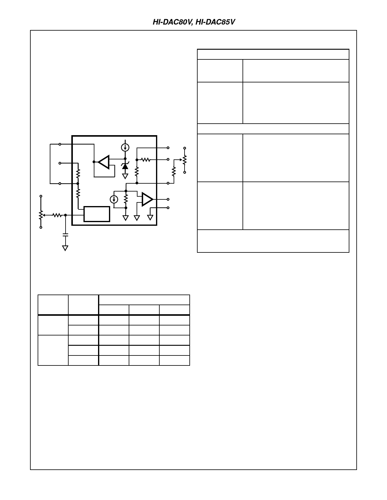
FIGURE 2. HI-DAC80V
18
+VS
19
R2
3.9
MΩ
20
15
-VS
5kΩ
TO
100kΩ
21
14
24
16
21
22
18
19
20
-
15
+
Unipolar
Bipolar
TABLE 2. RANGE CONNECTIONS
CONNECT
RANGE
PIN 15
PIN 17
0 to +5V
18
NC
0 to +10V
18
NC
±2.5V
18
20
±5V
18
20
±10V
19
20
PIN 19
20
NC
20
NC
15
FIGURE 1.
Reference Supply
An internal 6.3V reference is provided on board the
HI-DAC80V. The voltage (pin 24) is accurate to ±0.8% and
must be connected to the reference input (pin 16) for
specified operation. This reference may be used externally,
provided current drain is limited to 2.5mA. An external buffer
amplifier is recommended if this reference is to be used to
drive other system components. Otherwise, variations in the
load driven by the reference will result in gain variations of
the HI-DAC80V. All gain adjustments should be made under
constant load conditions.
TABLE 3. GAIN AND OFFSET CALIBRATIONS
UNIPOLAR CALIBRATION
Step 1:
Offset
Turn all bits OFF (11 . . . 1)
Adjust R2 for 0V out
Step 2:
Gain
Turn all bits ON (00 . . . 0)
Adjust R1 for FS - 1 LSB
That is:
4.9988 for 0 to +5V range
9.9976 for 0 to +10V range
BIPOLAR CALIBRATION
Step 1:
Offset
Turn all bits OFF (11 . . . 1)
Adjust R2 for Negative FS
That is:
-10V for ±10V range
-5V for ±5V range
-2.5V for ±2.5V range
Step 2:
Gain
Turn all bits ON (00 . . . 0)
Adjust R1 for Positive FS - 1 LSB
That is:
+9.9951V for ±10V Range
+4.9976V for ±5V Range
+2.4988V for ±2.5V Range
This Bipolar procedure adjusts the output range end points. The
maximum error at zero (half scale) will not exceed the Linearity
Error. See the “Accuracy” Specifications.
6
Share Link: 