HI-DAC80V(2001) Просмотр технического описания (PDF) - Intersil
Номер в каталоге
Компоненты Описание
Список матч
HI-DAC80V Datasheet PDF : 8 Pages
| |||
HI-DAC80V
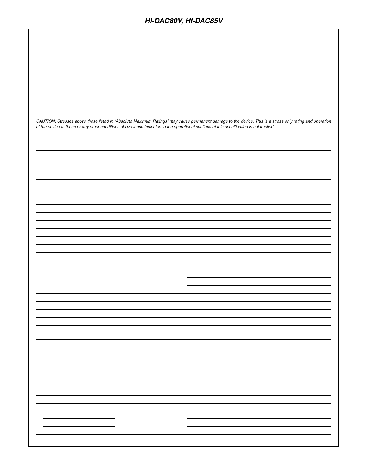
Absolute Maximum Ratings
Power Supply Inputs
+VS. . . . . . . . . . . . . . . . . . . . . . . . . . . . . . . . . . . . . . . . . . . . +20V
-VS . . . . . . . . . . . . . . . . . . . . . . . . . . . . . . . . . . . . . . . . . . . . . -20V
Reference
Input (Pin 16) . . . . . . . . . . . . . . . . . . . . . . . . . . . . . . . . . . . . . +VS
Output Drain . . . . . . . . . . . . . . . . . . . . . . . . . . . . . . . . . . . . 2.5mA
Digital Inputs (Bits 1 to 12). . . . . . . . . . . . . . . . . . . . . . . . -1V to +VS
Operating Conditions
Temperature Range . . . . . . . . . . . . . . . . . . . . . . . . . . . . 0oC to 75oC
Thermal Information
Thermal Resistance (Typical, Note 1)
θJA (oC/W)
PDIP Package . . . . . . . . . . . . . . . . . . . . . . . . . . . . .
55
Maximum Power Dissipation
PDIP Package . . . . . . . . . . . . . . . . . . . . . . . . . . . . . . . . . 550mW
Maximum Junction Temperature . . . . . . . . . . . . . . . . . . . . . . 150oC
Maximum Storage Temperature Range . . . . . . . . . . -65oC to 150oC
Maximum Lead Temperature (Soldering 10s) . . . . . . . . . . . . 300oC
Die Characteristics
Process . . . . . . . . . . . . . . . . . . . . . . . . . . . . . . . . . . . . . . . Bipolar-DI
Transistor Count. . . . . . . . . . . . . . . . . . . . . . . . . . . . . . . . . . . . . . 214
CAUTION: Stresses above those listed in “Absolute Maximum Ratings” may cause permanent damage to the device. This is a stress only rating and operation of the
device at these or any other conditions above those indicated in the operational sections of this specification is not implied.
NOTE:
1. θJA is measured with the component mounted on a low effective thermal conductivity test board in free air. See Tech Brief TB379 for details.
Electrical Specifications TA = 25oC, VS ±12V to ±15V (Note 5), Pin 16 Shorted to Pin 24, Unless Otherwise Specified
PARAMETER
TEST CONDITIONS
MIN
TYP
MAX
UNITS
SYSTEM PERFORMANCE
Resolution
-
-
12
Bits
ACCURACY (Note 3)
Linear Error
Differential Linearity Error
Monotonicity
Full Temperature
Full Temperature
Full Temperature
-
±1/4
±1/2
LSB
-
±1/2
±3/4
LSB
Guaranteed
Gain Error
Full Temperature (Notes 2, 4)
-
±0.1
±0.3
% FSR
Offset Error
Full Temperature (Note 2)
±0.05
±0.15
% FSR
ANALOG OUTPUT
Output Ranges (See Figure 2 and
Table 2)
-
±2.5
-
V
-
±5
-
V
-
±10
-
V
-
0 to 5
-
V
-
0 to 10
-
V
Output Current
±5
-
-
mA
Output Resistance
-
0.05
-
Ω
Short Circuit Duration
To Common
Continuous
-
DRIFT (Note 3)
Total Bipolar Drift (Includes Gain,
Offset and Linearity Drifts)
Full Temperature
-
-
±20
ppm/oC
Total Error
Unipolar
Full Temperature (Note 6)
-
±0.08
±0.15
% FSR
Bipolar
Gain
Full Temperature (Note 6)
With Internal Reference
Without Internal Reference
-
±0.06
±0.1
% FSR
-
±15
±30
ppm/oC
-
±7
-
ppm/oC
3
Share Link: 