HI5805EVAL1(1999) Просмотр технического описания (PDF) - Intersil
Номер в каталоге
Компоненты Описание
Список матч
HI5805EVAL1 Datasheet PDF : 12 Pages
| |||
HI5805
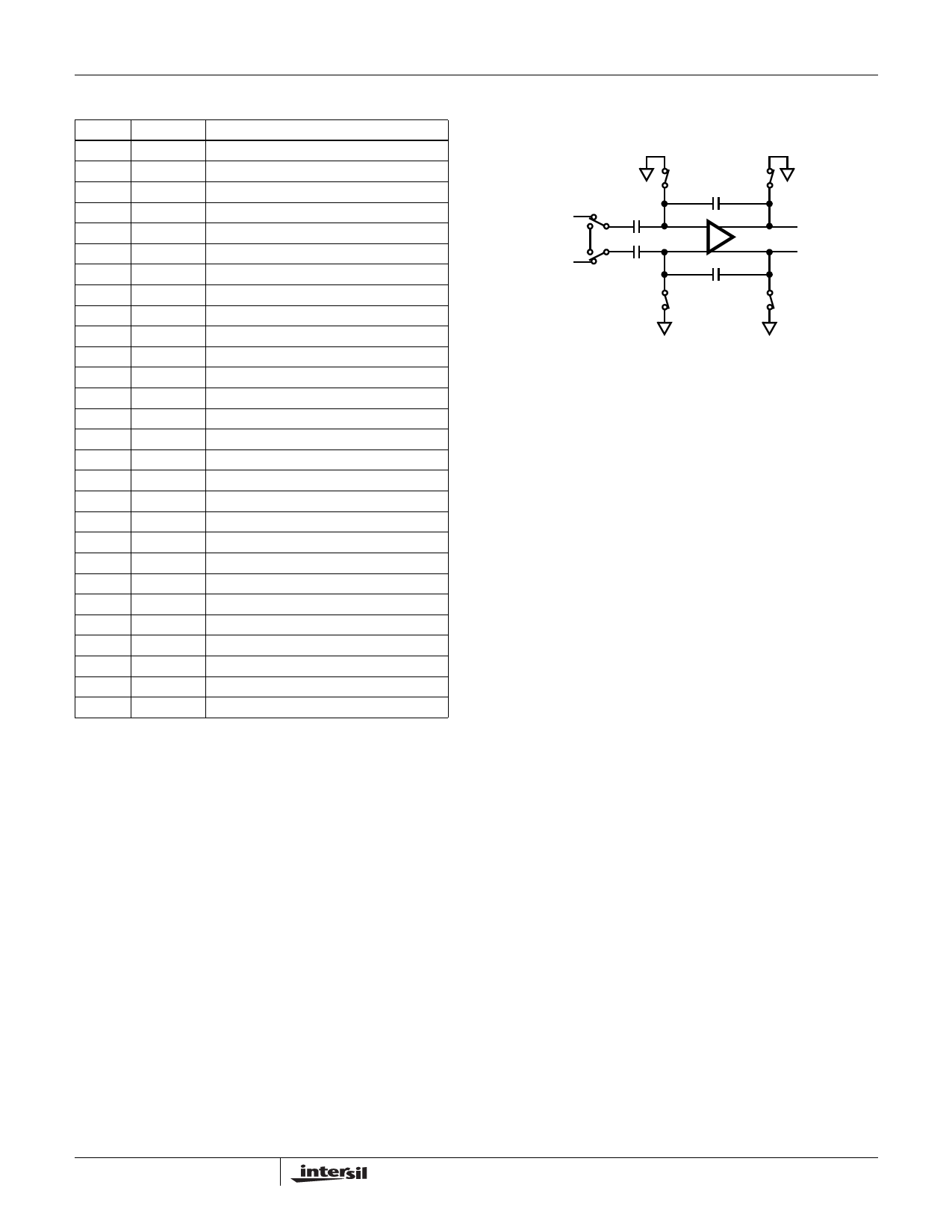
Pin Descriptions
PIN NO.
1
2
3
4
5
6
7
8
9
10
11
12
13
14
15
16
17
18
19
20
21
22
23
24
25
26
27
28
NAME
CLK
DVCC1
DGND1
DVCC1
DGND1
AVCC
AGND
VIN+
VIN-
VDC
VROUT
VRIN
AGND
AVCC
D11
D10
D9
D8
D7
D6
DGND2
DVCC2
D5
D4
D3
D2
D1
D0
DESCRIPTION
Input Clock.
Digital Supply (5.0V).
Digital Ground.
Digital Supply (5.0V).
Digital Ground
Analog Supply (5.0V).
Analog Ground.
Positive Analog Input.
Negative Analog Input.
DC Bias Voltage Output.
Reference Voltage Output.
Reference Voltage Input.
Analog Ground.
Analog Supply (5.0V).
Data Bit 11 Output (MSB).
Data Bit 10 Output.
Data Bit 9 Output.
Data Bit 8 Output.
Data Bit 7 Output.
Data Bit 6 Output.
Digital Output Ground.
Digital Output Supply (3.0V to 5.0V).
Data Bit 5 Output.
Data Bit 4 Output.
Data Bit 3 Output.
Data Bit 2 Output.
Data Bit 1 Output.
Data Bit 0 Output (LSB).
Detailed Description
Theory of Operation
The HI5805 is a 12-bit, fully-differential, sampling pipeline A/D
converter with digital error correction. Figure 14 depicts the
circuit for the front end differential-in-differential-out sample-
and-hold (S/H). The switches are controlled by an internal
clock which is a non-overlapping two phase signal, f1 and f2,
derived from the master clock. During the sampling phase, f1,
the input signal is applied to the sampling capacitors, CS. At
the same time the holding capacitors, CH, are discharged to
analog ground. At the falling edge of f1 the input signal is
sampled on the bottom plates of the sampling capacitors. In
the next clock phase, f2, the two bottom plates of the sampling
capacitors are connected together and the holding capacitors
are switched to the op-amp output nodes. The charge then
redistributes between CS and CH completing one sample-
and-hold cycle. The output is a fully-differential, sampled-data
representation of the analog input. The circuit not only
performs the sample-and-hold function but will also convert a
single-ended input to a fully-differential output for the
converter core. During the sampling phase, the VIN pins see
only the on-resistance of a switch and CS. The relatively small
values of these components result in a typical full power input
bandwidth of 100MHz for the converter.
φ1
VIN +
CS
φ2
φ 1 CH
-
+
+-
VIN -
φ1
CS
φ1
CH
φ1
VOUT +
VOUT-
φ1
FIGURE 14. ANALOG INPUT SAMPLE-AND-HOLD
As illustrated in the functional block diagram and the timing
diagram in Figure 1, three identical pipeline subconverter
stages, each containing a four-bit flash converter, a four-bit
digital-to-analog converter and an amplifier with a voltage
gain of 8, follow the S/H circuit with the fourth stage being
only a 4-bit flash converter. Each converter stage in the
pipeline will be sampling in one phase and amplifying in the
other clock phase. Each individual sub-converter clock
signal is offset by 180 degrees from the previous stage
clock signal, with the result that alternate stages in the
pipeline will perform the same operation.
The 4-bit digital output of each stage is fed to a digital delay
line controlled by the internal clock. The purpose of the delay
line is to align the digital output data to the corresponding
sampled analog input signal. This delayed data is fed to the
digital error correction circuit which corrects the error in the
output data with the information contained in the redundant
bits to form the final 12-bit output for the converter.
Because of the pipeline nature of this converter, the data on
the bus is output at the 3rd cycle of the clock after the analog
sample is taken. This delay is specified as the data latency.
After the data latency time, the data representing each
succeeding sample is output at the following clock pulse. The
output data is synchronized to the external clock by a latch.
The digital outputs are in offset binary format (See Table 1).
Internal Reference Generator, VROUT and VRIN
The HI5805 has an internal reference generator, therefore, no
external reference voltage is required. VROUT must be
connected to VRIN when using the internal reference voltage.
The HI5805 can be used with an external reference. The
converter requires only one external reference voltage
connected to the VRIN pin with VROUT left open.
The HI5805 is tested with VRIN equal to 3.5V. Internal to the
converter, two reference voltages of 1.3V and 3.3V are
generated for a fully differential input signal range of ±2V.
In order to minimize overall converter noise, it is
recommended that adequate high frequency decoupling be
provided at the reference voltage input pin, VRIN.
123
Share Link: 