HI5805EVAL1(1999) Просмотр технического описания (PDF) - Intersil
Номер в каталоге
Компоненты Описание
Список матч
HI5805EVAL1 Datasheet PDF : 12 Pages
| |||
HI5805
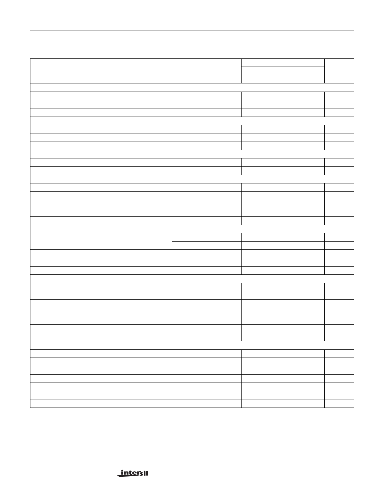
Electrical Specifications
TAAVC=C-4=0oDCVCtoC815=oCD,VDCiCff2er=enDtViaCl AC3na=lo+g5I.n0pVu, tf,ST=yp5iMcaSl PVaSluaets50a%re
Duty
Test
RCeysculelt,sVaRt I2N5=oC3,.5V,
CL
=
10pF,
Unless Otherwise Specified (Continued)
HI5805BIB (-40oC TO 85oC)
PARAMETER
TEST CONDITION
MIN
TYP
MAX
UNITS
INTERNAL VOLTAGE REFERENCE
Reference Output Voltage, VROUT (Loaded)
Reference Output Current
Reference Temperature Coefficient
-
3.5
-
V
-
-
1
mA
-
200
-
ppm/oC
REFERENCE VOLTAGE INPUT
Reference Voltage Input, VRIN
Total Reference Resistance, RL
Reference Current
-
3.5
-
V
-
7.8
-
kΩ
-
450
-
µA
DC BIAS VOLTAGE
DC Bias Voltage Output, VDC
Max Output Current (Not To Exceed)
-
2.3
-
V
-
-
1
mA
DIGITAL INPUTS (CLK)
Input Logic High Voltage, VIH
Input Logic Low Voltage, VIL
Input Logic High Current, IIH
Input Logic Low Current, IIL
Input Capacitance, CIN
DIGITAL OUTPUTS (D0-D11)
VCLK = 5V
VCLK = 0V
2.0
-
-
V
-
-
0.8
V
-
-
10.0
µA
-
-
10.0
µA
-
7
-
pF
Output Logic Sink Current, IOL
Output Logic Source Current, IOH
Output Capacitance, COUT
TIMING CHARACTERISTICS
VO = 0.4V (Note 2)
1.6
-
-
mA
DVCC3 = 3.0V, VO = 0.4V
-
1.6
-
mA
VO = 2.4V (Note 2)
-0.2
-
-
mA
DVCC3 = 3.0V, VO = 2.4V
-
-0.2
-
mA
-
5
-
pF
Aperture Delay, tAP
Aperture Jitter, tAJ
Data Output Delay, tOD
Data Output Hold, tH
Data Latency, tLAT
Clock Pulse Width (Low)
-
-
-
-
For a Valid Sample (Note 2)
-
5MSPS Clock
90
5
-
ns
5
-
ps (RMS)
8
-
ns
8
-
ns
-
3
Cycles
100
110
ns
Clock Pulse Width (High)
5MSPS Clock
90
100
110
ns
POWER SUPPLY CHARACTERISTICS
Total Supply Current, ICC
Analog Supply Current, AICC
Digital Supply Current, DICC1
Output Supply Current, DICC2
Power Dissipation
Offset Error PSRR, ∆VOS
Gain Error PSRR, ∆FSE
NOTES:
VIN+ - VIN- = 2V
-
60
70
mA
VIN+ - VIN- = 2V
-
46
-
mA
VIN+ - VIN- = 2V
-
13
-
mA
VIN+ - VIN- = 2V
-
1
-
mA
VIN+ - VIN- = 2V
-
300
350
mW
AVCC or DVCC = 5V ±5%
-
2
-
LSB
AVCC or DVCC = 5V ±5%
-
30
-
LSB
2. Parameter guaranteed by design or characterization and not production tested.
3. With the clock off (clock low, hold mode).
119
Share Link: 