AD9432 Просмотр технического описания (PDF) - Analog Devices
Номер в каталоге
Компоненты Описание
Список матч
AD9432 Datasheet PDF : 20 Pages
| |||
AD9432
APPLICATION NOTES
Theory of Operation
The AD9432 is a multibit pipeline converter that uses a switched
capacitor architecture. Optimized for high speed, this converter
provides flat dynamic performance up to frequencies near Nyquist.
DNL transitional errors are calibrated at final test to a typical
accuracy of 0.25 LSB or less.
USING THE AD9432
Analog Input
The analog input to the AD9432 is a differential buffer. The input
buffer is self-biased by an on-chip resistor divider that sets the
dc common-mode voltage to a nominal 3 V (see Equivalent
Circuits section). Rated performance is achieved by driving the
input differentially. Minimum input offset voltage is obtained when
driving from a source with a low differential source impedance
such as a transformer in ac applications. Capacitive coupling at the
inputs will increase the input offset voltage by as much as ± 25 mV.
Driving the ADC single-endedly will degrade performance.
For best dynamic performance, impedances at AIN and AIN
should match.
Special care was taken in the design of the analog input section
of the AD9432 to prevent damage and corruption of data when
the input is overdriven. The nominal input range is 2 V p-p.
Each analog input will be 1 V p-p when driven differentially.
PECL
GATE
510⍀
0.1F
510⍀ 0.1F
AD9432
ENCODE
ENCODE
GND
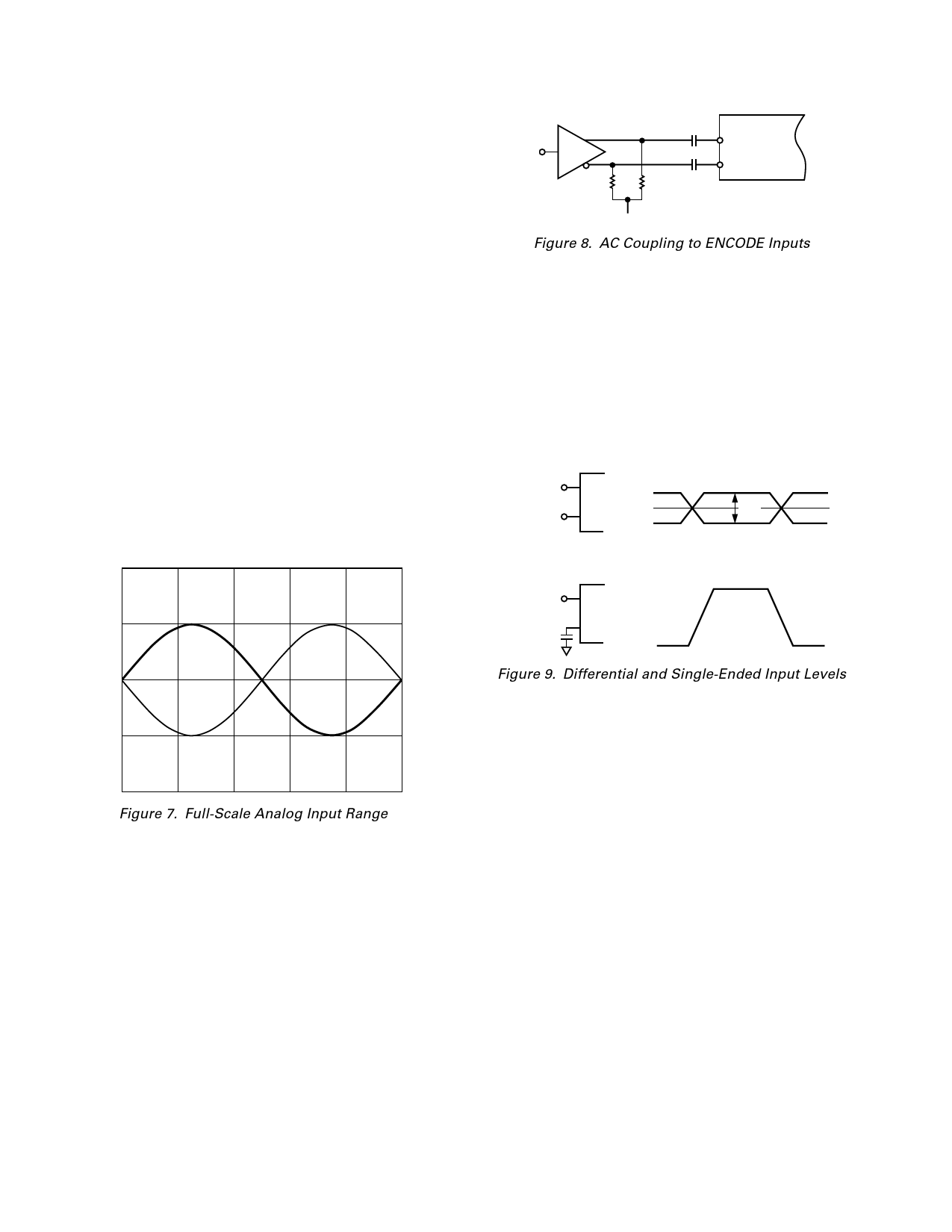
Figure 8. AC Coupling to ENCODE Inputs
ENCODE Voltage Level Definition
The voltage level definitions for driving ENCODE and ENCODE
in single-ended and differential mode are shown in Figure 9.
ENCODE Inputs
Differential Signal Amplitude (VID) . . . . . . . . . . . 500 mV min
. . . . . . . . . . . . . . . . . . . . . . . . . . . . . . . . . . . . . . 750 mV nom
High Differential Input Voltage (VIHD) . . . . . . . . . . 3.5 V max
Low Differential Input Voltage (VILD) . . . . . . . . . . . . . 0 V min
Common-Mode Input (VICM) . . . . . . . 1.25 V min, 1.6 V nom
High Single-Ended Voltage (VIHS) . . . . . 2 V min to 3.5 V max
Low Single-Ended Voltage (VILS) . . . . . 0 V min to 0.8 V max
ENCODE
VIHD
ENCODE
VICM
VILD
VID
4.0
AIN
3.5
3.0
AIN
2.5
2.0
Figure 7. Full-Scale Analog Input Range
ENCODE Input
Any high speed A/D converter is extremely sensitive to the qual-
ity of the sampling clock provided by the user. A track/hold
circuit is essentially a mixer, and any noise, distortion, or timing
jitter on the clock will be combined with the desired signal at the
A/D output. For that reason, considerable care has been taken
in the design of the ENCODE input of the AD9432, and the
user is advised to give commensurate thought to the clock source.
The ENCODE input supports either differential or single-ended
and is fully TTL/CMOS compatible.
Note that the ENCODE inputs cannot be driven directly from
PECL level signals (VIHD is 3.5 V max). PECL level signals can
easily be accommodated by ac coupling as shown in Figure 8.
Good performance is obtained using an MC10EL16 in the
circuit to drive the encode inputs.
ENCODE
VIHS
0.1F
VILS
Figure 9. Differential and Single-Ended Input Levels
Often, the cleanest clock source is a crystal oscillator producing
a pure sine wave. In this configuration, or with any roughly
symmetrical clock input, the input can be ac-coupled and biased
to a reference voltage that also provides the ENCODE. This
ensures that the reference voltage is centered on the encode signal.
Digital Outputs
The digital outputs are 3.3 V (2.7 V to 3.6 V) TTL/CMOS-
compatible for lower power consumption. The output data
format is Two’s Complement, illustrated in Table I. The out of
range (OR) output (logic LOW for normal operation) will be
HIGH during any clock cycle when the ADC output data (Dx)
reach positive or negative full scale (–2048 or +2047). The OR
is internally generated each clock cycle, has the same pipe-
line latency and propagation delay as the ADC output data, and
will remain HIGH until the output data reflect an in-range
condition. The ADC output bits (Dx) will not roll over, and
will therefore remain at positive or negative full scale (+2048 or
–2047) while the OR output is HIGH.
–10–
REV. E
Share Link: 