CXA1744AR Просмотр технического описания (PDF) - Sony Semiconductor
Номер в каталоге
Компоненты Описание
Список матч
CXA1744AR Datasheet PDF : 18 Pages
| |||
CXA1744AR
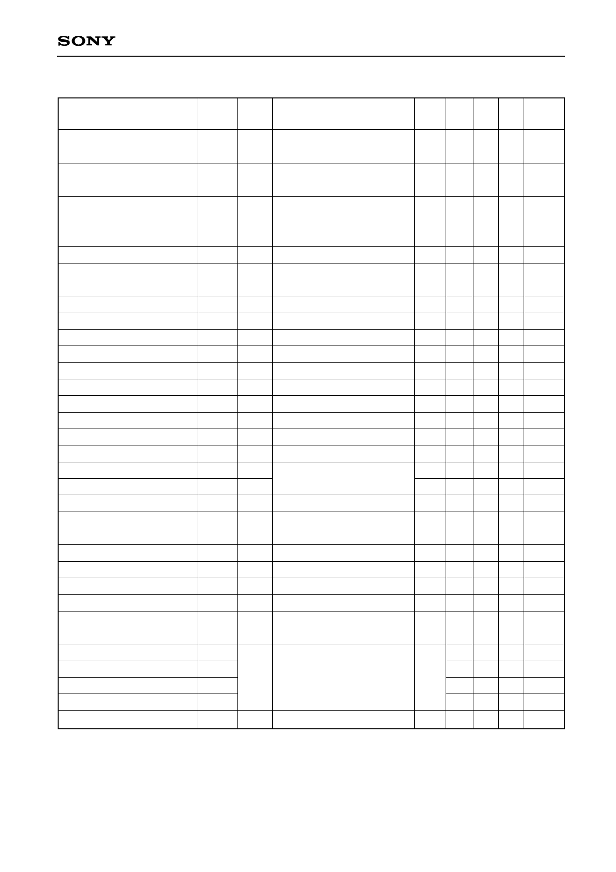
Electrical Characteristics (VCC=3.0V, Ta=25°C, refer to the Electrical Characteristics Measurement Circuit)
Item
Symbol SW set Measurement conditions
Min. Typ. Max. Unit
to ON
For operating
Current consumption 1
ICC
VIN7=10MHz, 0dBm
I7 6.4 8.4 11.2 mA
Current consumption 2
For power saving
ICC
S1
VIN7=10MHz, 0dBm
VIN5=150.05MHz, -40dBm
I7 — 0.2 0.5 mA
Mixer conversion gain
GVMIX
VIN6=139.35MHz, -10dBm
RL=330Ω
Mixer output resistance
ROMIX
IF AMP voltage gain
VIN4=10.7MHz, -60dBm
GIF S10
RL=470Ω
IF AMP input resistance
RIIF
IF AMP output resistance
ROIF
Limiter voltage gain
GLIM
VIN3=10.7MHz, -80dBm
Limiter input resistance
RILIM
Limiter output voltage amplitude VLIM
VIN3=10.7MHz, -20dBm
V3 15.5 18 20.5 dB
240 330 420
Ω
V2 31 33.5 36
dB
240 330 420
320 440 560
24pin 64 66.5 69
340 460 580
24pin 320 400 480
Ω
Ω
dB
Ω
mVP-P
RSSI output current inclination (IF)
VIN4=10.7MHz, -30~0dBm
I8 0.32 0.4 0.54 µA/dB
RSSI output current inclination (LIM)
RSSI dynamic range
DRSSI
VIN3=10.7MHz, -45~-15dBm
For MIXIN input
I8 0.32 0.4 0.54 µA/dB
75 80 —
dB
RSSI relative precision
— — ±3
dB
RSSI output voltage range
0.2 — 1.3
V
Detector output voltage
Detector total harmonic distortion
VDET
THD
VIN3=10.7MHz, -20dBm
FMOD=36kHz, fDEV=±25kHz
V1 160 200 240 mVrms
V1 — — 3.0
%
Detector maximum output voltage
1.2 — — VP-P
Detector output voltage High level
VCC — —
V
-1.1
Detector output voltage Low level
— — 0.5
V
REG1 output voltage
VREG1 S9 IL=300µA
20pin 1.07 1.17 1.27 V
COMP1 output saturation voltage ISAT1 S2 VIN1=1.1V, Isink=5mA
COMP1 output leak current
ILEAK1
3pin — 0.35 0.5
V
I1 — — 1.0 µA
COMP1 input bias current
S3 Measured value/2
IB1
S4
I2 -200 -70 —
nA
COMP1 rise time
COMP1 fall time
COMP1 rise propagation delay time
COMP1 fall propagation delay time
tr1
tf1
tpdr1
tpdf1
VIN1=DC level 1.3V
— 70 200
Rectangular wave of 100kHz, 0.5VP-P
— 40 200
3pin
RL=1KΩ, CL=20PF
— 130 500
— 160 500
nsec
nsec
nsec
nsec
COMP1 input dynamic range
For Vref=1.3V
0.3 — VCC
V
—8—
Share Link: 