CXA1744AR Просмотр технического описания (PDF) - Sony Semiconductor
Номер в каталоге
Компоненты Описание
Список матч
CXA1744AR Datasheet PDF : 18 Pages
| |||
CXA1744AR
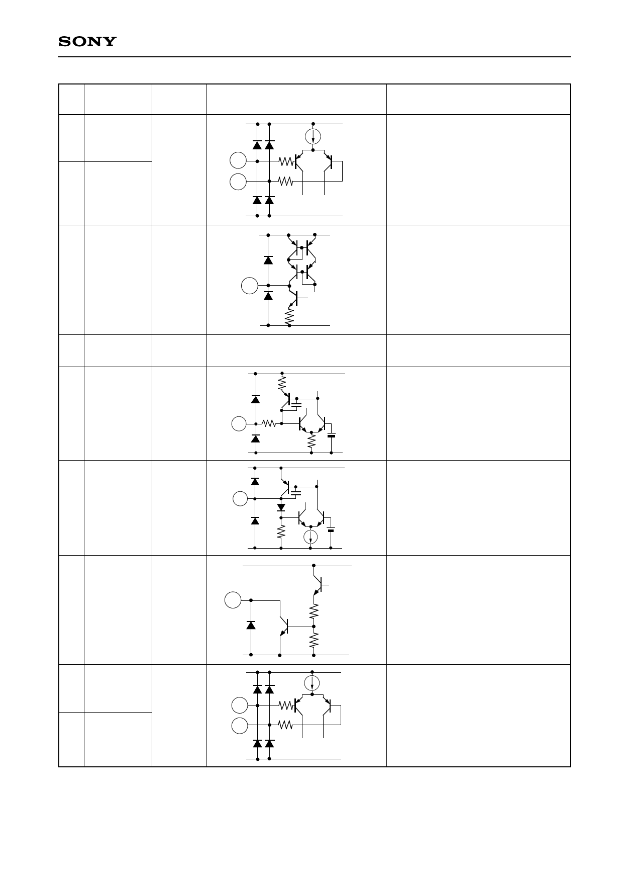
Pin
No.
Symbol
Typical pin
voltage
10 ICOMPIN
—
11 ICOMPINX
12 ICOMPOUT
—
Equivalent circuit
VCC
129
10
129
11
Description
Sample-and-hold circuit input.
ICOMPIN is for in-phase input.
ICOMPINX is for out-of-phase input.
GND
VCC
Sample-and-hold circuit output.
12
13
GND
14 CURREF
0V
1.25V
15
VREF
1.9V
129
14
15
16 FCOMPOUT —
16
GND
VCC
1.25V
GND
VCC
GND for circuits other than the MIX,
OSC, MULTI, and RSSI circuits.
Adjustment for RSSI output current.
Connects a resistor between this pin
and GND.
Reference voltage.
Leave this pin open normally.
1.25V
GND
VCC
Comparator output for free-channel
detection.
17 FCOMPINX
—
18 FCOMPIN
129
17
129
18
GND
VCC
Comparator input for free-channel
detection.
FCOMPINX is for out-of-phase input.
FCOMPIN is for in-phase input.
GND
—4—
Share Link: 