HM62W4100H Просмотр технического описания (PDF) - Hitachi -> Renesas Electronics
Номер в каталоге
Компоненты Описание
Список матч
HM62W4100H Datasheet PDF : 13 Pages
| |||
HM62W4100H Series
AC Characteristics (Ta = 0 to +70°C, VCC = 3.3 V ± 0.3 V, unless otherwise noted.)
Test Conditions
• Input pulse levels: 3.0 V/0.0 V
• Input rise and fall time: 3 ns
• Input and output timing reference levels: 1.5 V
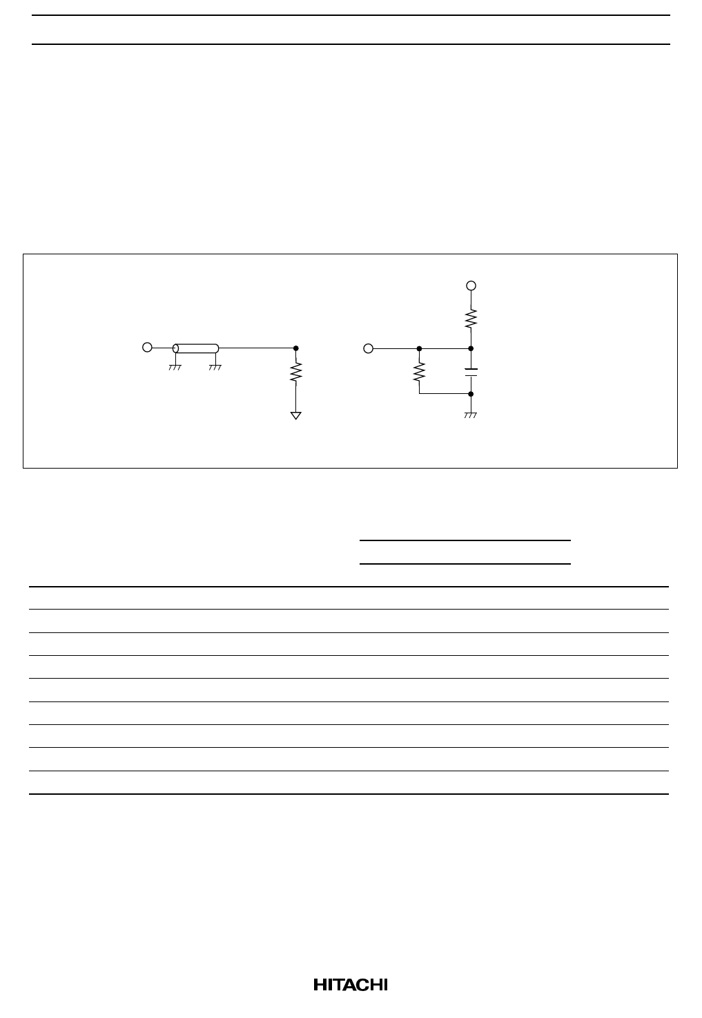
• Output load: See figures (Including scope and jig)
3.3 V
Dout Zo=50 Ω
RL=50 Ω
Dout
353 Ω
319Ω
5 pF
1.5 V
Output load (A)
Output load (B)
(for tCLZ, tOLZ, tCHZ, tOHZ, tWHZ, and tOW)
Read Cycle
Parameter
Read cycle time
Address access time
Chip select access time
Output enable to outpput valid
Output hold from address change
Chip select to output in low-Z
Output enable to output in low-Z
Chip deselect to output in high-Z
Output disable to output in high-Z
Symbol
t RC
t AA
t ACS
t OE
t OH
t CLZ
t OLZ
t CHZ
t OHZ
HM62W4100H
-12
-15
Min Max Min
12
—
15
—
12
—
—
12
—
—
6
—
3
—
3
3
—
3
0
—
0
—
6
—
—
6
—
Max Unit Notes
—
ns
15
ns
15
ns
7
ns
—
ns
—
ns
1
—
ns
1
7
ns
1
7
ns
1
6
Share Link: 