ISPGDX240VA-7B388I Даташит - Lattice Semiconductor
Description
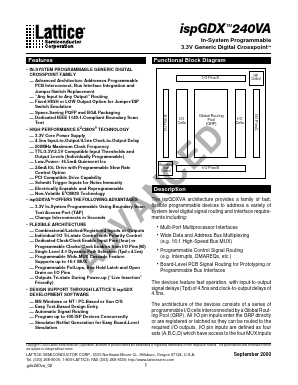
The ispGDXVA architecture provides a family of fast, flexible programmable devices to address a variety of system-level digital signal routing and interface requirements including:
• Multi-Port Multiprocessor Interfaces
• Wide Data and Address Bus Multiplexing (e.g. 16:1 High-Speed Bus MUX)
• Programmable Control Signal Routing (e.g. Interrupts, DMAREQs, etc.)
• Board-Level PCB Signal Routing for Prototyping or Programmable Bus Interfaces
The devices feature fast operation, with input-to-output signal delays (Tpd) of 4.5ns and clock-to-output delays of 4.5ns.
FEATUREs
• IN-SYSTEM PROGRAMMABLE GENERIC DIGITAL CROSSPOINT FAMILY
— Advanced Architecture Addresses Programmable PCB Interconnect, Bus Interface Integration and Jumper/Switch Replacement
— “Any Input to Any Output” Routing
— Fixed HIGH or LOW Output Option for Jumper/DIP Switch Emulation
— Space-Saving PQFP and BGA Packaging
— Dedicated IEEE 1149.1-Compliant Boundary Scan Test
• HIGH PERFORMANCE E2CMOS® TECHNOLOGY
— 3.3V Core Power Supply
— 4.5ns Input-to-Output/4.5ns Clock-to-Output Delay
— 200MHz Maximum Clock Frequency
— TTL/3.3V/2.5V Compatible Input Thresholds and Output Levels (Individually Programmable)
— Low-Power: 16.5mA Quiescent Icc
— 24mA IOL Drive with Programmable Slew Rate Control Option
— PCI Compatible Drive Capability
— Schmitt Trigger Inputs for Noise Immunity
— Electrically Erasable and Reprogrammable
— Non-Volatile E2CMOS Technology
• ispGDXVA™ OFFERS THE FOLLOWING ADVANTAGES
— 3.3V In-System Programmable Using Boundary Scan Test Access Port (TAP)
— Change Interconnects in Seconds
• FLEXIBLE ARCHITECTURE
— Combinatorial/Latched/Registered Inputs or Outputs
— Individual I/O Tri-state Control with Polarity Control
— Dedicated Clock/Clock Enable Input Pins (four) or Programmable Clocks/Clock Enables from I/O Pins (60)
— Single Level 4:1 Dynamic Path Selection (Tpd = 4.5ns)
— Programmable Wide-MUX Cascade Feature Supports up to 16:1 MUX
— Programmable Pull-ups, Bus Hold Latch and Open Drain on I/O Pins
— Outputs Tri-state During Power-up (“Live Insertion” Friendly)
• DESIGN SUPPORT THROUGH LATTICE’S ispGDX DEVELOPMENT SOFTWARE
— MS Windows or NT / PC-Based or Sun O/S
— Easy Text-Based Design Entry
— Automatic Signal Routing
— Program up to 100 ISP Devices Concurrently
— Simulator Netlist Generation for Easy Board-Level Simulation
