STLC1511 Просмотр технического описания (PDF) - STMicroelectronics
Номер в каталоге
Компоненты Описание
Список матч
STLC1511 Datasheet PDF : 31 Pages
| |||
STLC1511
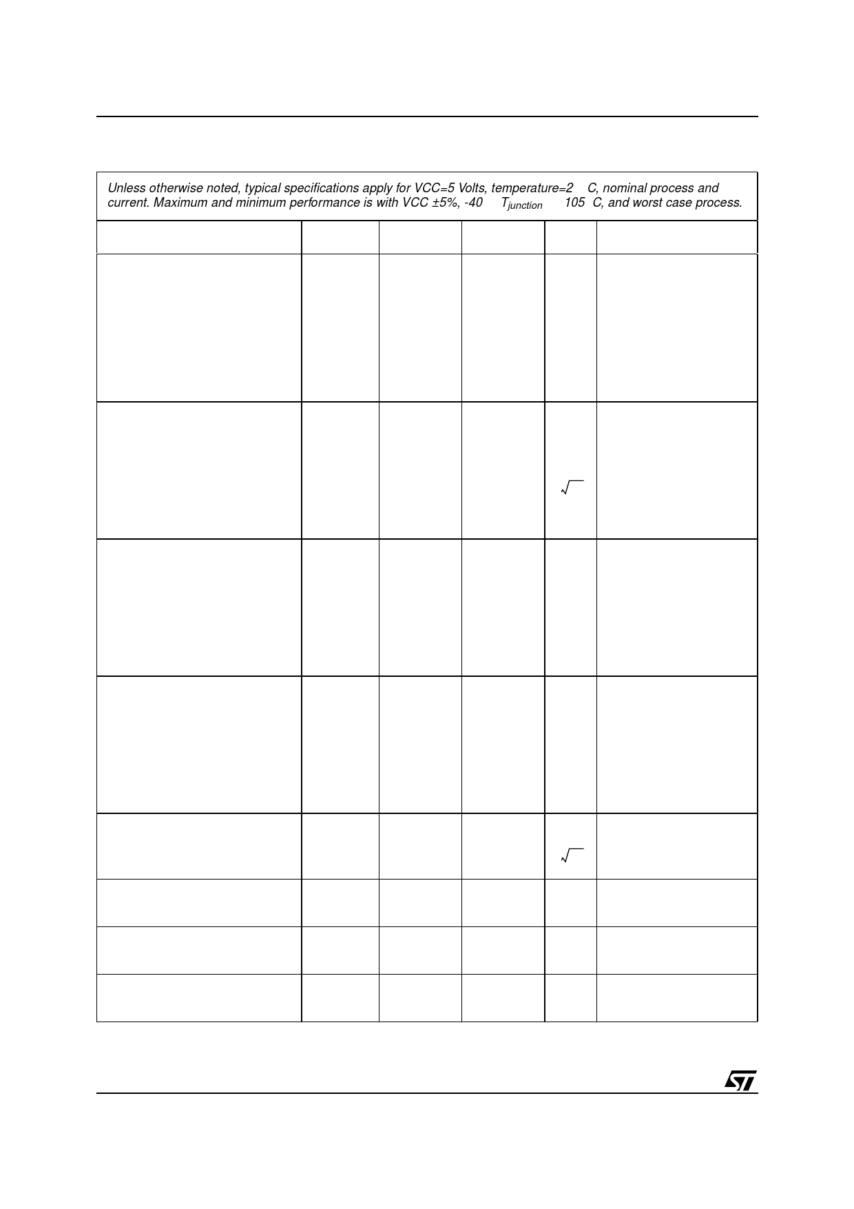
Table 3. Transmit Path Specifications
Unless otherwise noted, typical specifications apply for VCC=5 Volts, temperature=27×C, nominal process and
current. Maximum and minimum performance is with VCC ±5%, -40 =<Tjunction =< 105×C, and worst case process.
Description
min
typ
max
Units
Comments
Output Signal to Distortion ratio
Two tone7
DS Multi-tone8
75
81
30kHz =< f =< 120kHz
155kHz =< f =< 540kHz
US Multi-tone9
78
84
76
82
30kHz =< f =< 120kHz
155kHz =< f =< 540kHz
78
84
78
84
For all TxPGA gains.
dB
Measured differentially at
TXOP/N
Output Referred Noise Voltage
10 11 12
TxPGA Gain = 0dB
30kHz =< f =< 120kHz
155kHz =< f =< 540kHz
TxPGA Gain = min
30kHz =< f =< 120kHz
155kHz =< f =< 540kHz
80
80
100
100
---n---V----
measured differentially at
TXOP/N
Hz
30
40
30
40
Output Signal to Noise and
Distortion Ratio (DS) 13 14
TxPGA Gain = 0dB
30kHz =< f =< 120kHz
155kHz =< f =< 540kHz
74
80
73
79
TxPGA Gain = min
30kHz =< f =< 120kHz
155kHz =< f =< 540kHz
53
59
53
59
measured differentially at
dB
TXOP/N
Output Signal to Noise and
Distortion Ratio (US) 15 13
TxPGA Gain = 0dB
30kHz =< f =< 120kHz
155kHz =< f =< 540kHz
76
82
76
82
TxPGA Gain = min
30kHz =< f =< 120kHz
155kHz =< f =< 540kHz
55
61
55
61
measured differentially at
dB
TXOP/N
Out of Band Noise
72
---n---V----
band from 550KHz - 2.2
MHz (fS/2)
Hz
Maximum Output Signal
@TXOP/N
Load Resistance @ pin TXOP/N
500
Load Capacitance @ pin TXOP/
N
2.4
Vp
differential output
per output to 2.5V
W
per output to 2.5V
10
pF
10/31
Share Link: 