CDB5394 Просмотр технического описания (PDF) - Cirrus Logic
Номер в каталоге
Компоненты Описание
Список матч
CDB5394 Datasheet PDF : 22 Pages
| |||
CS5394
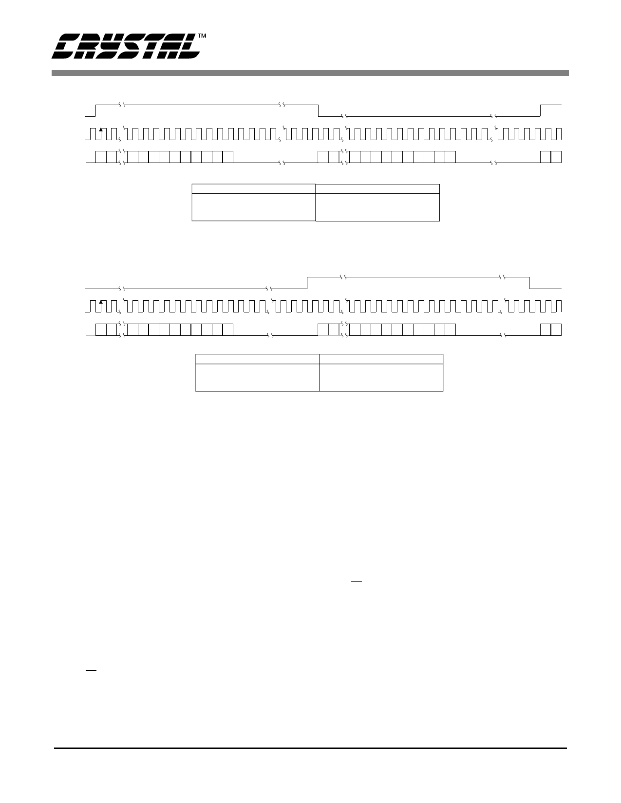
LRCK
Left Channel
SCLK
SDATA
23 22 9 8 7 6 5 4 3 2 1 0
Right Channel
23 22 9 8 7 6 5 4 3 2 1 0
MASTER
24-Bit Left Justified Data
Data Valid on Rising Edge of 64x SCLK
MCLK equal to 256x Fs
SLAVE
24-Bit Left Justified Data
Data Valid on Rising Edge of SCLK
MCLK equal to 256x Fs
Figure 2. Serial Data Format, DFS Low
23 22
LRCK
Left Channel
SCLK
SDATA
23 22 9 8 7 6 5 4 3 2 1 0
Right Channel
23 22 9 8 7 6 5 4 3 2 1 0
23 22
MASTER
I 2S 24-Bit Data
Data Valid on Rising Edge of 64x SCLK
MCLK equal to 256x Fs
SLAVE
I 2S 24-Bit Data
Data Valid on Rising Edge of SCLK
MCLK equal to 256x Fs
Figure 3. Serial Data Format, DFS High (I2S compatible)
Left / Right Clock
The Left/Right clock, LRCK, determines which
channel, left or right, is to be output on SDATA. In
Master Mode, LRCK is an output whose frequency
is equal to Fs. In Slave Mode, LRCK is an input
whose frequency must be equal to Fs and synchro-
nous to MCLKA/D.
Master Mode
In Master mode, SCLK and LRCK are outputs
which are internally derived from the master clock.
Internal dividers will divide MCLKA/D by 4 to
generate a SCLK which is 64× Fs and by 256 to
generate a LRCK which is equal to Fs. The CS5394
is placed in the Master mode with the slave/master
pin, S/M, low.
Slave Mode
LRCK and SCLK become inputs in slave mode.
LRCK must be externally derived from MCLKA/D
and be equal to Fs. It is recommended that SCLK
be equal to 64×. Other frequencies between 48×
and 128× Fs are possible but may degrade system
performance due to interference effects. The mas-
ter clock frequency must be 256× Fs. The CS5394
is placed in the Slave mode with the slave/master
pin, S/M, high.
Analog Connections
Figure 1 shows the analog input connections. The
analog inputs are presented differentially to the
modulators via the AINR+/- and AINL+/- pins.
Each analog input will accept a maximum of
2.0 Vpp. The + and - input signals are 180° out of
phase resulting in a differential input voltage of
4.0 Vpp. Figure 4 shows the input signal levels for
10
DS258PP4
Share Link: 