W78354P Просмотр технического описания (PDF) - Winbond
Номер в каталоге
Компоненты Описание
Список матч
W78354P Datasheet PDF : 44 Pages
| |||
W78C354
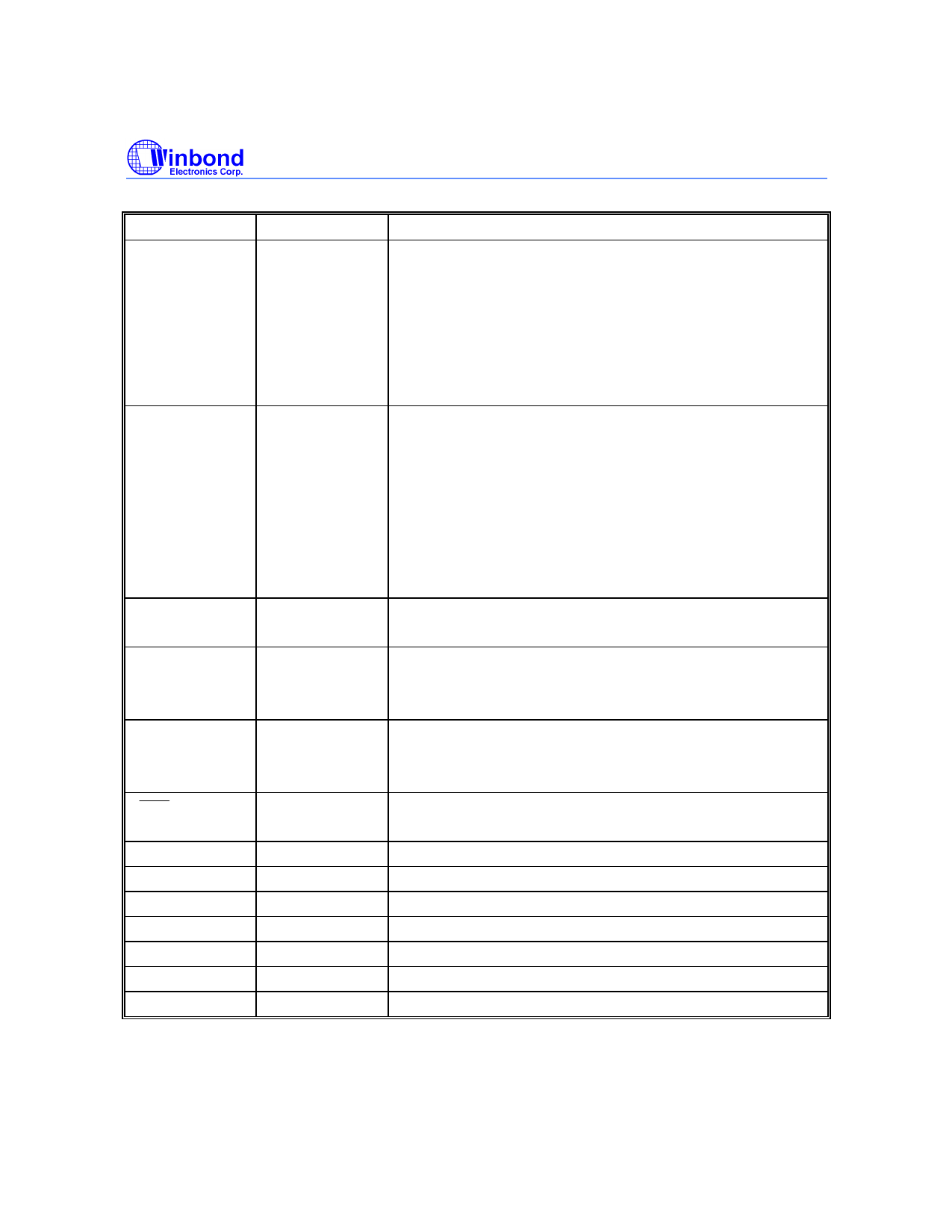
Pin Description, continued
PIN NAME
P2.2
P2.3 (STP)
P2.4 (SDAC10)
P2.5 (SDAC11)
P2.6 (SDAC12)
P2.7 (SDAC13)
I/O TYPE
I/O
P3.0 (RXD)
I/O
P3.1 (TXD)
P3.2 (INT0)
P3.3
P3.4 (T0)
P3.5 (T1)
P3.6
P3.7
P4.0−P4.6
O
HIN
I
VIN
HOUT
O
VOUT
RST
I
OSCOUT
O
OSCIN
I
VPP
I
VDD
I
VSS
I
VAA
I
VSSA
I
BLOCK DIAGRAM
FUNCTION
General purpose I/O.
Sink/source current 4 mA/-100 µA.
Alternate function:
P2.3: STP (Self-Test Pattern) output.
P2.4−P2.7: SDAC10−13 outputs.
While outputing special function, P2.3−P2.7 sink/source
current is 4 mA/-4 mA.
General purpose I/O.
Sink/Source current 2 mA/-100 µA.
Alternate function:
P3.0: Serial input port.
P3.1: Serial output port.
P3.2: External interrupt input.
P3.4, P3.5: Timer/counter 0, 1 external inputs.
Output port.
Sink/source current 2 mA/-2 mA.
HIN: Hsync/composite sync input.
VIN: Vsync input.
Schmitt trigger input pin.
HOUT: Hsync output.
VOUT: Vsync output.
Sink/source current 4 mA/-4 mA.
Reset the controller (active low).
Schmitt trigger input pin.
Output from inverting oscillator amplifier.
Input to inverting oscillator amplifier.
High voltage supply input for flash PROM.
Positive power supply for digital circuit, +5V.
Digital ground.
Positive power supply for analog circuit, +5V.
Analog ground.
Publication Release Date: October 1996
-5-
Revision A1
Share Link: 