LTC2873H Просмотр технического описания (PDF) - Analog Devices
Номер в каталоге
Компоненты Описание
Список матч
LTC2873H Datasheet PDF : 32 Pages
| |||
LTC2873
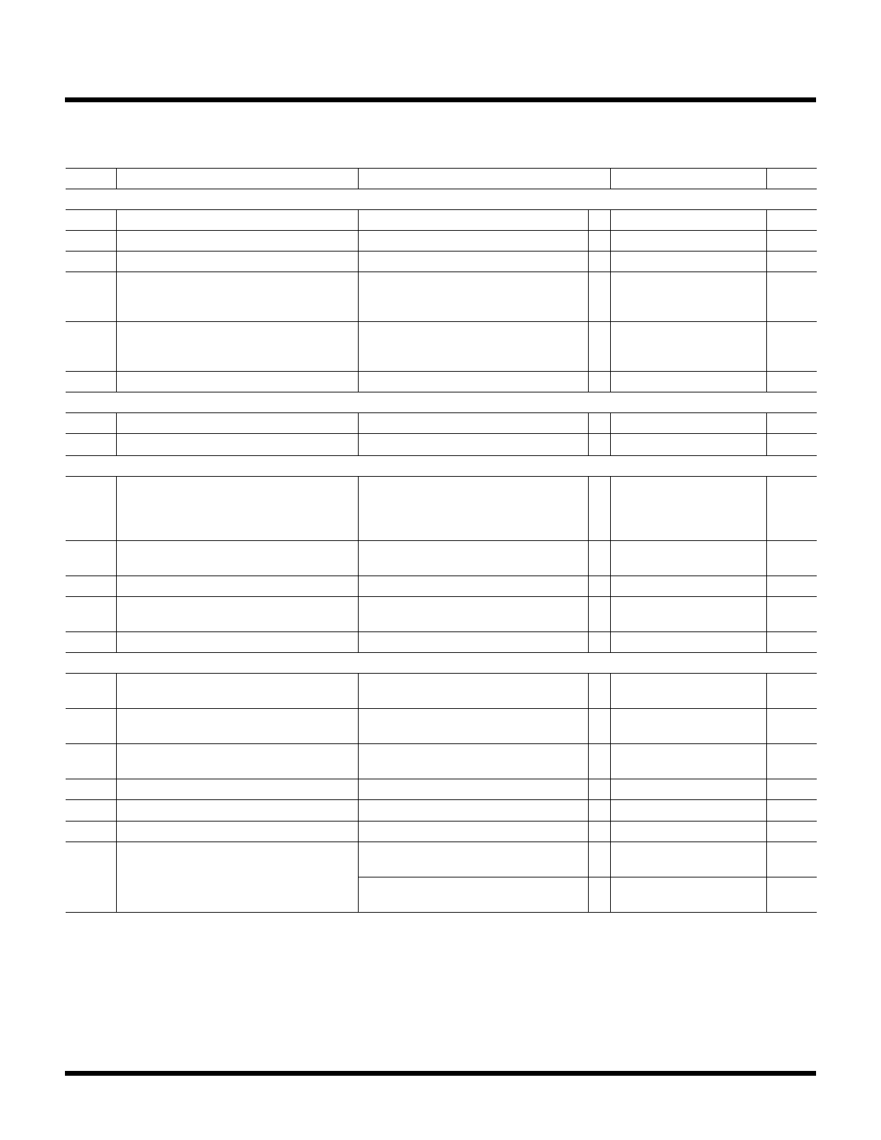
ELECTRICAL CHARACTERISTICS The l denotes the specifications which apply over the full operating
temperature range, otherwise specifications are at TA = 25°C. VCC = VL = 3.3V, TE485 = VL, LB = 0V unless otherwise noted. (Notes 2, 6)
SYMBOL PARAMETER
CONDITIONS
MIN TYP MAX
Supplies
VCC
Supply Voltage Operating Range
l3
5.5
VL
Logic Supply Voltage Operating Range
VL ≤ VCC
l 1.7
VCC
VCC Supply Current in Shutdown Mode
SHDN = 0V
l
8
30
VCC Supply Current in RS232 Mode or
RS485 Mode, Driver and Receiver Enabled,
Termination Disabled
No Load, SHDN = TE485 = DE485/F232 = VL l
RE485 = 0
4
9
VCC Supply Current in RS485 Mode with
No Load, SHDN = 485/232 = VL
l
Receiver and Termination Enabled, Driver
DE485/F232 = RE485 = TE485 = 0
Disabled
4
9
VL Supply Current in Any Mode
Power Supply Generator
No Load
l
0
5
VDD
Regulated VDD Output Voltage
SHDN = VL, No Load
7.0
VEE
Regulated VEE Output Voltage
SHDN = VL, No Load
–6.3
RS485 Driver
|VOD|
Differential Output Voltage
RL = Open, VCC = 3V (Figure 1)
l
VCC
RL = 27Ω, VCC = 4.5V (Figure 1)
l 2.1
VCC
RL = 27Ω, VCC = 3V (Figure 1)
l 1.5
VCC
RL = 50Ω, VCC = 3.13V (Figure 1)
l2
∆|VOD| Difference in Magnitude of Differential Output RL = 27Ω, VCC = 3V (Figure 1)
l
0.2
Voltage for Complementary Output States
RL = 50Ω, VCC = 3.13V (Figure 1)
l
0.2
VOC
Common Mode Output Voltage
RL = 27Ω or 50Ω (Figure 1)
l
3
∆|VOC| Difference in Magnitude of Common Mode Output RL = 27Ω or 50Ω (Figure 1)
l
0.2
Voltage for Complementary Output States
IOSD485 Maximum Short-Circuit Current
–7V ≤ VOUT ≤ 12V (Figure 2)
l
±250
RS485 Receiver
IIN485
RIN485
Input Current (A/DO, B/RI)
Input Resistance (A/DO, B/RI)
Differential Input Signal Threshold
Voltage (A/DO to B/RI)
(A/DO or B/RI) = 12V or –7V,
VCC = 0V or 3.3V (Figure 3)
(A/DO or B/RI) = 12V or –7V,
VCC = 0V or 3.3V (Figure 3)
–7V ≤ (A/DO or B/RI) ≤ 12V
l –100
125
125
l
±200
Input Hysteresis
B = 0V
220
Differential Input Failsafe Rising Threshold Voltage –7V ≤ (A/DO or B/RI) ≤ 12V, (A/D0 – B/RI) Rising l –200 –70
–20
Input DC Failsafe Hysteresis
40
VOL
Receiver Output Low Voltage
Output Low, I(RO) = 3mA (Sinking),
l
0.4
3V ≤ VL ≤ 5.5V
Output Low, I(RO) = 1mA (Sinking),
l
0.4
1.7V ≤ VL < 3V
UNITS
V
V
µA
mA
mA
µA
V
V
V
V
V
V
V
V
V
mA
µA
kΩ
mV
mV
mV
mV
V
V
REV B
For more information www.analog.com
3
Share Link: 