PI74LPT16952V Просмотр технического описания (PDF) - Pericom Semiconductor
Номер в каталоге
Компоненты Описание
Список матч
PI74LPT16952V Datasheet PDF : 5 Pages
| |||
PI74LPT16952
1234567890123456789012345678901212345678901234567890123456789012123456789012334.536V789011623-4B56I7T890R12E12G345I6S78T90E12R34E56D789T01R234A56N78S90C12E12I3V456E78R90S12
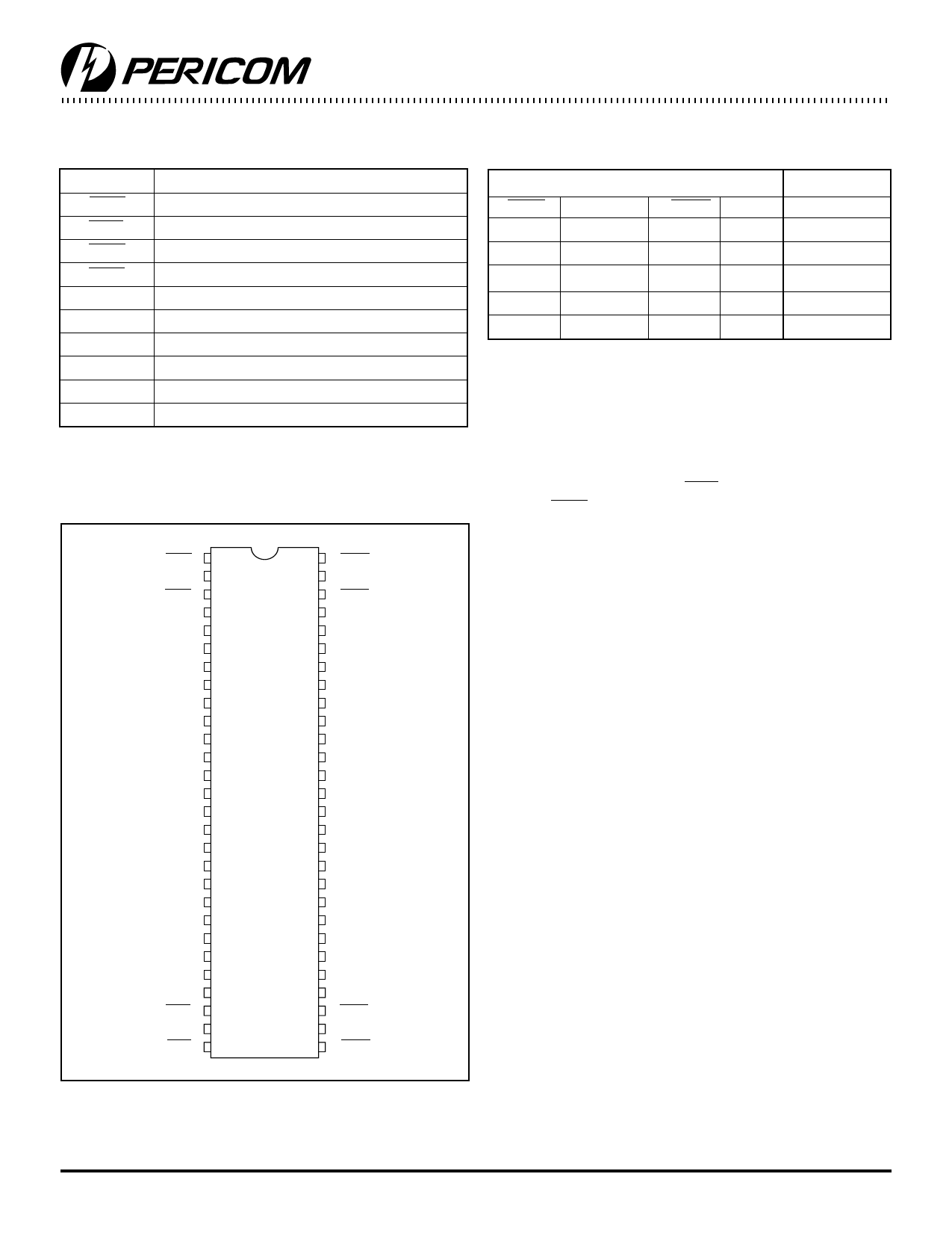
Product Pin Description
Pin Name
xOEAB
xOEBA
xCEAB
xCEBA
xCLKAB
xCLKBA
xAx
xBx
GND
VCC
Description
A-to-B Output Enable Input (Active LOW)
B-to-A Output Enable Input (Active LOW)
A-to-B Clock Enable Input (Active LOW)
B-to-A Clock Enable Input (Active LOW)
A-to-B Clock Input
B-to-A Clock Input
A-to-B Data Inputs or B-to-A 3-State Outputs
B-to-A Data Inputs or B-to-A 3-State Outputs
Ground
Power
Product Pin Configuration
1OEAB
1CLKAB
1CEAB
GND
1A0
1A1
VCC
1A2
1A3
1A4
GND
1A5
1A6
1A7
2A0
2A1
2A2
GND
2A3
2A4
2A5
VCC
2A6
2A7
GND
2CEAB
2CLKAB
2OEAB
1
56
2
55
3
54
4
53
5
52
6
51
7
50
8
49
9
48
10
47
11
46
12
45
13
44
14 56-PIN 43
15 V56 42
16 A56 41
17
40
18
39
19
38
20
37
21
36
22
35
23
34
24
33
25
32
26
31
27
30
28
29
1OEBA
1CLKBA
1CEBA
GND
1B0
1B1
VCC
1B2
1B3
1B4
GND
1B5
1B6
1B7
2B0
2B1
2B2
GND
2B3
2B4
2B5
VCC
2B6
2B7
GND
2CEBA
2CLKBA
2OEBA
Truth Table(1,2)
Inputs
XCEAB XCLKAB XOEAB XAX
H
X
L
X
X
L
L
X
L
↑
L
L
L
↑
L
H
X
X
H
X
Outputs
XBX
B(3)
B(3)
L
H
High Z
Notes:
1. H = High Voltage Level
L = Low Voltage Level
X = Don't Care or Irrelevant
↑ = LOW-to-HIGH Transition
Z = High Impedance
2. A-to-B data flow shown. B-to-A flow control
is the same, except using xCEBA, xCLKBA,
and xOEBA.
3. Level of B before the indicated steady-state
input conditions were established.
2
PS2076A 02/4/97
Share Link: 