PI5C16213 Просмотр технического описания (PDF) - Pericom Semiconductor
Номер в каталоге
Компоненты Описание
Список матч
PI5C16213 Datasheet PDF : 3 Pages
| |||
PI5C16213
1122334455667788990011223344556677889900112233445566778899001122112233445566778899001122334455667788990011223344556677889900112211223344556677889900112233445566778899001122334455667788990011221122334455667788990011223344556677889900112233445566778899001122112233445566778899001122
24-Bit Bus-Exchange Switch
Product Features:
• Near-zero propagation delay
• 5Ω switches connect inputs to outputs
• Direct bus connection when switches are ON
• Ultra-low quiescent power (0.2 µA typical)
– Ideally suited for notebook applications
• Industrial operating temperature: –40°C to +85°C
• Packages available:
– 56-pin 240-mil wide thin plastic TSSOP (A)
– 56-pin 300-mil wide plastic SSOP (V)
Product Description:
Pericom Semiconductor’s PI5C series of logic circuits are pro-
duced in the Company’s advanced 0.6 micron CMOS technology.
The PI5C16213 is a 24-bit bus-exchange switch designed with a
low ON resistance allowing connections to be made with minimal
propagation delay. This device operates as a 24-bit or a 12-bit bus
switch, which provides data exchanging between the four signal
ports via the data-select (S0-S2) terminals.
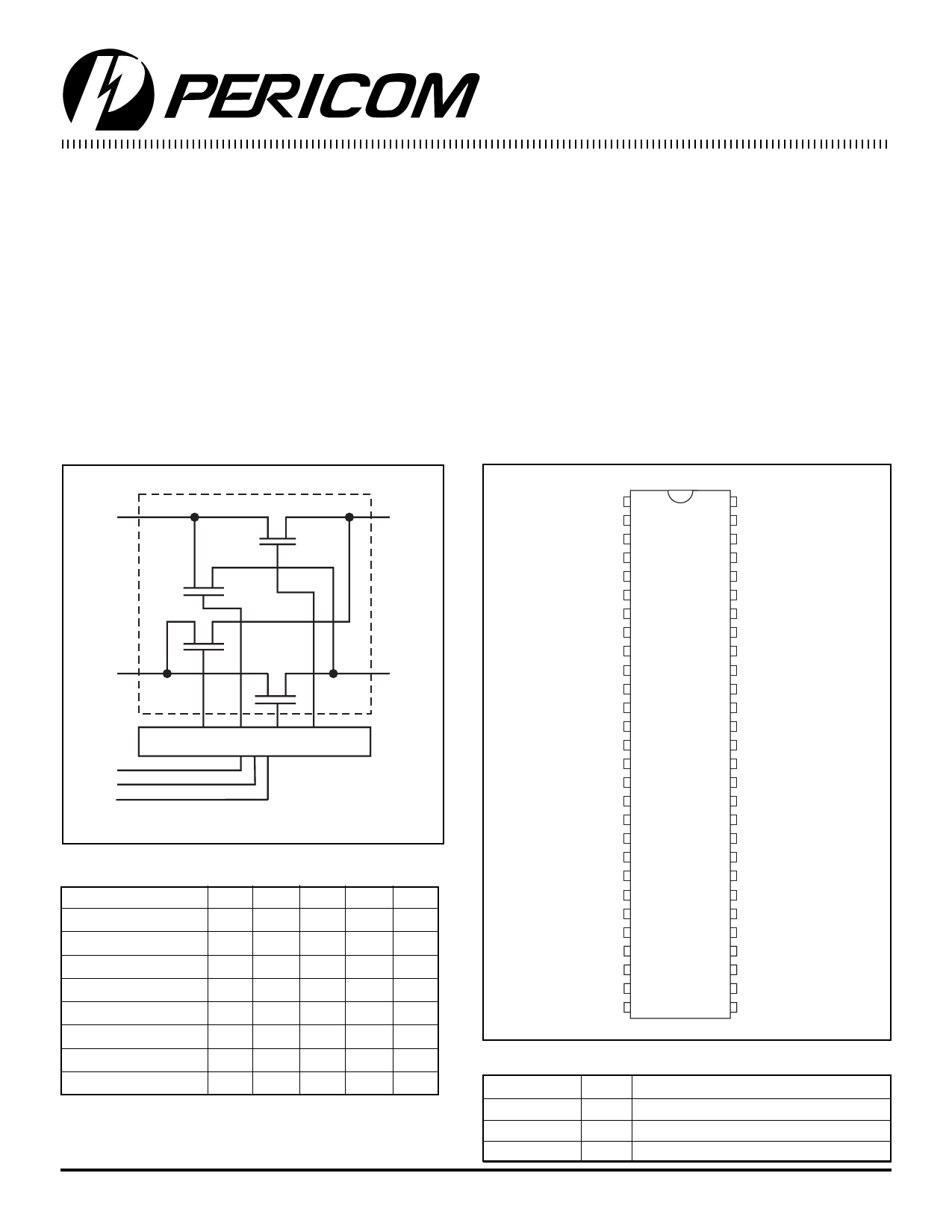
Logic Block Diagram
Product Pin Configuration
1 of 12 Channels
1A1
1B1
1A2
1B2
Flow Control
S0
S1
S2
Truth Table
Function
S2 S1
Disconnect
LL
A1 to B1
LL
A1 to B2
LH
A2 to B1
LH
A2 to B2
HL
A1 to A2 and B2
HL
A1 to B1, A2 to B2 H H
A1 to B2, A2 to B1 H H
NOTE: 1. H = High Voltage Level
L = Low Voltage Level
Z = High Impedance
S0 A1 A2
LZZ
H B1 Z
L B2 Z
H Z B1
L Z B2
H A2/B2 Z
L B1 B2
H B2 B1
S0
1A1
1A2
2A1
2A2
3A1
3A2
GND
4A1
4A2
5A1
5A2
6A1
6A2
7A1
7A2
VCC
8A1
GND
8A2
9A1
9A2
10A1
10A2
11A1
11A2
12A1
12A2
1
56
2
55
3
54
4
53
5
52
6
51
7
50
8
49
9
48
10 56-PIN 47
11 A, V 46
12
45
13
44
14
43
15
42
16
41
17
40
18
39
19
38
20
37
21
36
22
35
23
34
24
33
25
32
26
31
27
30
28
29
S1
S2
1B1
1B2
2B1
2B2
3B1
GND
3B2
4B1
4B2
5B1
5B2
6B1
6B2
7B1
7B2
8B1
GND
8B2
9B1
9B2
10B1
10B2
11B1
11B2
12B1
12B2
Product Pin Description
Pin Name I/O
S0-S2
I
xAx
I/O
xBx
I/O
Description
Select Inputs
Bus A
Bus B
116
PS7051A 08/12/96
Share Link: 