CY7C109BL-15ZC Просмотр технического описания (PDF) - Cypress Semiconductor
Номер в каталоге
Компоненты Описание
Список матч
CY7C109BL-15ZC Datasheet PDF : 12 Pages
| |||
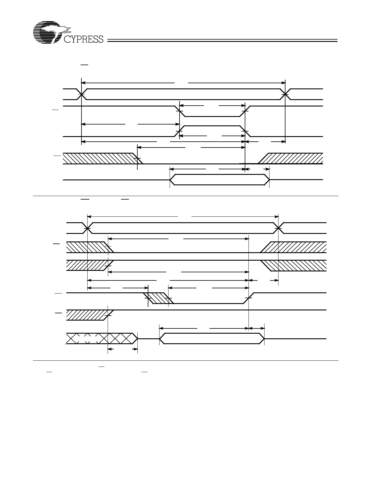
Switching Waveforms (continued)
Write Cycle No. 1 (CE1 or CE2 Controlled)[13, 14]
ADDRESS
CE1
CE2
WE
DATA I/O
tSA
tAW
tWC
tSCE
tPWE
tSCE
tSD
DATA VALID
Write Cycle No. 2 (WE Controlled, OE HIGH During Write)[13, 14]
ADDRESS
CE1
tWC
tSCE
CE2
WE
tSCE
tAW
tSA
tPWE
tHA
tHD
tHA
CY7C109B
CY7C1009B
109B–9
OE
DATA I/O
NOTE 15
tHZOE
tSD
tHD
DATAIN VALID
Notes:
13. Data I/O is high impedance if OE = VIH.
14. If CE1 goes HIGH or CE2 goes LOW simultaneously with WE going HIGH, the output remains in a high-impedance state.
15. During this period the I/Os are in the output state and input signals should not be applied.
109B–10
Document #: 38-05038 Rev. **
Page 7 of 12
Share Link: 