LTC1235CSW Просмотр технического описания (PDF) - Linear Technology
Номер в каталоге
Компоненты Описание
Список матч
LTC1235CSW Datasheet PDF : 16 Pages
| |||
LTC1235
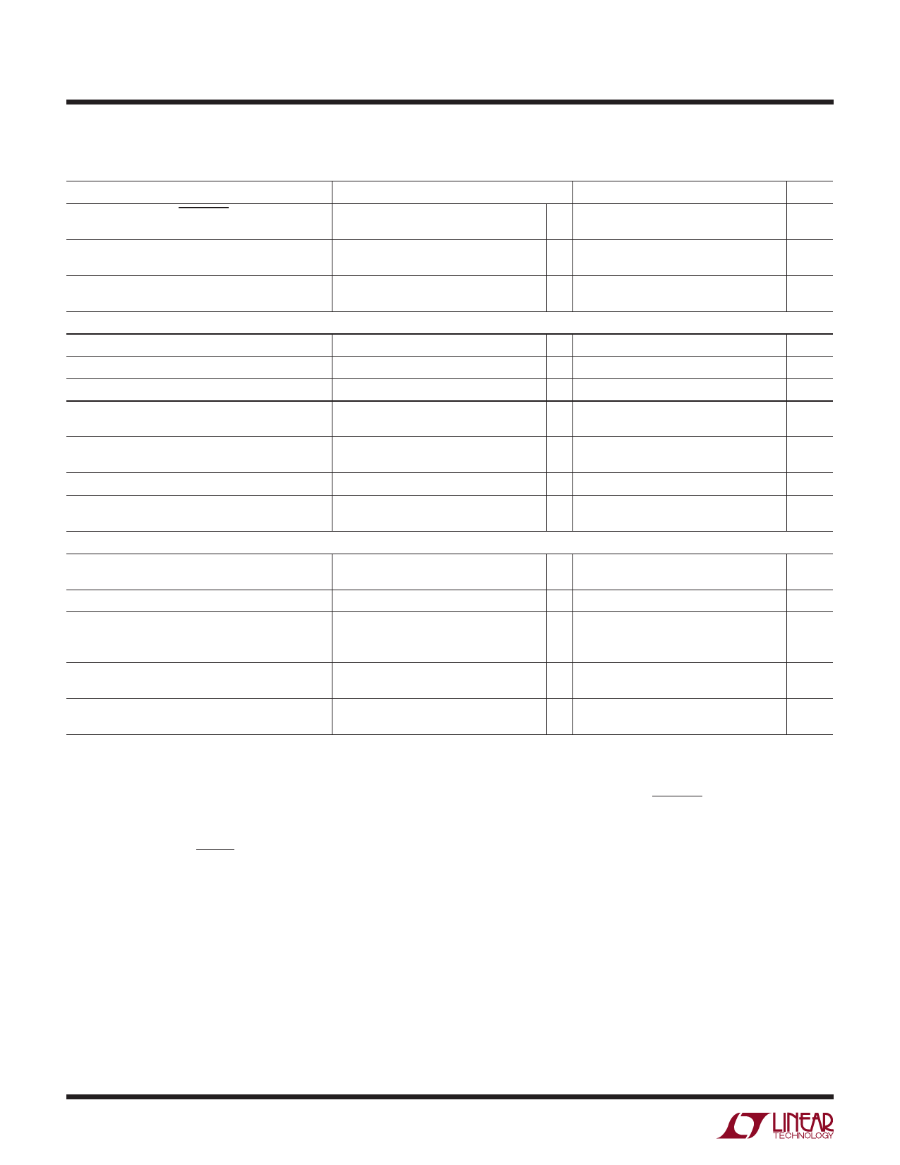
ELECTRICAL CHARACTERISTICS The l denotes the specifications which apply over the full operating
temperature range, otherwise specifications are at TA = 25°C. VCC = Full Operating Range, VBATT = 2.8V, Backup = No Connection,
TA = 25°C, unless otherwise noted.
PARAMETER
RESET, RESET, WDO, LOW LINE
Output Short Circuit Current (Note 6)
CONDITIONS
Output Source Current
Output Sink Current
MIN
TYP
MAX
UNITS
1
3
25
μA
25
mA
WDI Input Threshold
Logic Low
Logic High
0.8
V
2.0
V
WDI Input Current
WDI = VOUT
WDI = 0V
l
4
50
μA
l
–50
–8
μA
Power Fail Detector
PFI Input Threshold
VCC = 5V
l
1.25
1.3
1.35
V
PFI Input Threshold PSRR
0.3
mV/V
PFI Input Current
PFO Output Voltage (Note 6)
PFO Short Circuit Source Current
(Note 6)
PFI Comparator Response Time (falling)
PFI Comparator Response Time (rising)
(Note 6)
ISINK = 3.2mA
ISOURCE = 1A
PFI = HIGH, PFO = 0V
PFI = LOW, PFO = VOUT
ΔVIN = –20mV, VOD = 15mV
ΔVIN = 20mV, VOD = 15mV
with 10kΩ Pullup
±0.01
±25
nA
0.4
V
3.5
V
1
3
25
μA
30
mA
2
μs
40
μs
8
μs
Chip Enable Gating
CE IN Threshold
CE IN Pullup Current (Note 4)
CE OUT Output Voltage
CE Propagation Delay
CE OUT Output Short Circuit Current
VIL
VIH
ISINK = 3.2mA
ISOURCE = 3.0mA
ISOURCE = 1μA, VCC = 0V
VCC = 5V, CL = 20pF
Output Source Current
Output Sink Current
0.8
V
2.0
V
3
μA
VOUT – 1.50
VOUT – 0.05
0.4
V
V
V
20
35
ns
l
20
45
ns
30
mA
35
mA
Note 1: Stresses beyond those listed under Absolute Maximum Ratings
may cause permanent damage to the device. Exposure to any Absolute
Maximum Rating condition for extended periods may affect device
reliability and lifetime.
Note 2: All voltage values are with respect to GND.
Note 3: For military temperature range parts, consult the factory.
Note 4: The input pins of PB RST, BACKUP and CE IN, have weak internal
pullups which pull to the supply when the input pins are floating.
Note 5: The LTC1235 can be programmed either to provide or not to
provide battery backup power to the VOUT pin during power failure.
The power down condition of VOUT is selected by the logic level of the
BACKUP pin which is latched internally when VCC falls through the reset
voltage threshold. If the latched logic level of the BACKUP pin is high,
VOUT will be in Battery Backup Mode and will be switched to VBATT when
VCC falls below VBATT. If the latched logic level of the BACKUP pin is low,
VOUT will be in Battery Saving Mode when VCC falls below VBATT.
Note 6: The output pins of BATT ON, LOW LINE, PFO, WDO, RESET and
RESET have weak internal pullups of typically 3A. However, external
pullup resistors may be used when higher speed is required.
Note 7: The push-button reset input requires an active low signal.
Internally, this input signal is debounced and timed for a minimum of
40ms. When this condition is satisfied, the reset outputs go to the active
states. The reset outputs will remain in active states for a minimum of
140ms from the moment the push-button reset input is released from
logic low level.
1235fa
4
Share Link: 