HMC981LP3E Просмотр технического описания (PDF) - Hittite Microwave
Номер в каталоге
Компоненты Описание
Список матч
HMC981LP3E Datasheet PDF : 17 Pages
| |||
v01.0411
HMC981LP3E
ACTIVE BIAS CONTROLLER
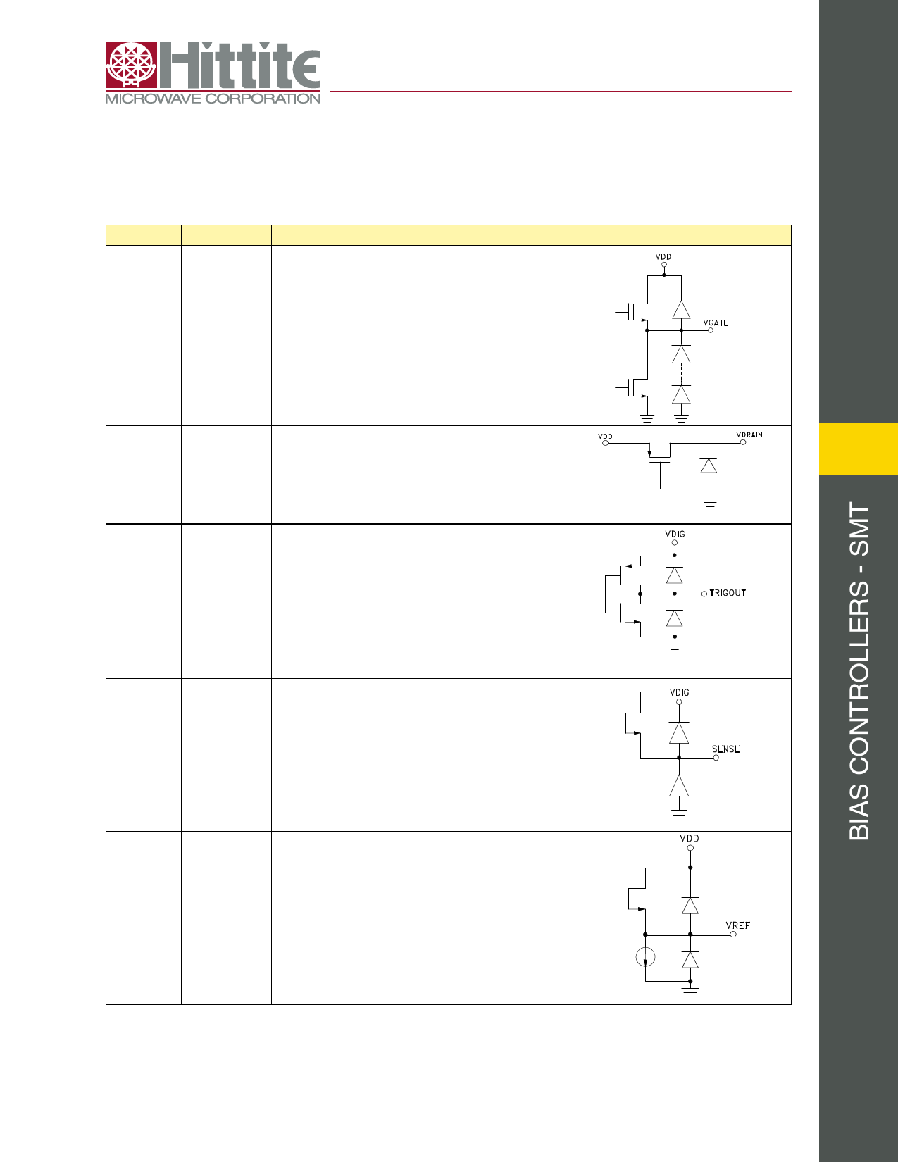
Pin Descriptions (Continued)
Pin Number
Function
Description
Gate Control pin for external amplifier. Connect to the gate
(base) of the external amplifier. In order to guarantee
11
VGATE
stability,a 10μF capacitor should be connected between
the gate (base) terminal of the external amplifier and GND
as close to the amplifier as possible.
Interface Schematic
Drain voltage. Should be connected to the supply
12
VDRAIN
terminal of the external amplifier. A minimum 100 nF
capacitor has to be placed close to the external amplifier to
improve load regulation.
13
Trigger out signal. Generates a HIGH (3.5V) signal when
13
TRIGOUT
the active bias system stabilizes. This signal can be
used to trigger next device (ENABLE) if more than one
HMC981LP3E is used in a daisy chain.
To adjust the bias current of the external amplifier connect
15
ISENSE
a resistor (Rsense) from ISENSE pin to GND. Use Eqn.2 to
determine the required Rsense value.
16
VREF
1.5V reference voltage. 0.1uF or greater capacitor to GND
is needed for noise filtering.
For price, delivery, and to place orders, please contact Hittite Microwave Corporation:
2 Elizabeth Drive, Chelmsford, MA 01824 Phone: 978-250-3343 Fax: 978-250-3373
Order On-line at www.hittite.com
13 - 8
Share Link: 